
At NVIDIA's GTC (the yearly GPU Technology Conference) in March, the company trumpeted its intentions to broadly supply the embedded market with Tegra SoCs and associated hardware and software development tools. As a specific example of this overarching strategy, NVIDIA unveiled a small form factor development kit called "Jetson TKI" (Figure 1), based on the ARM Cortex-A15-based "Logan" Tegra K1 application processor introduced in January at the Consumer Electronics Show (see sidebar "A Series of ARM-Based SoCs").
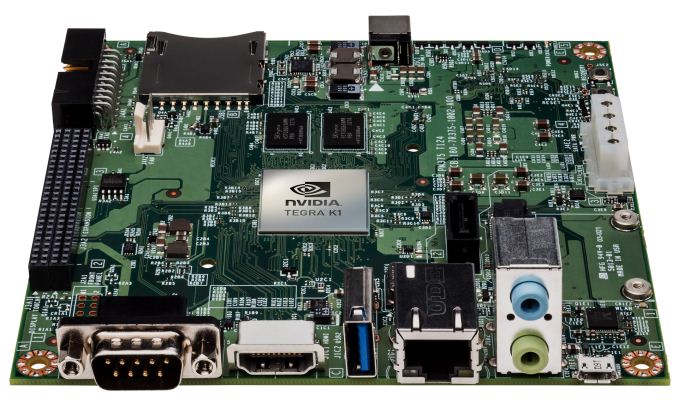
Figure 1. Jetson TK1 is touted as a comprehensive board-plus-software kit for developing Tegra K1-based computer vision and other applications.
Pre-orders for Jetson TK1 at $192 began at GTC, and kits will begin shipping concurrent with the publication of this article. The compact hardware system board is not based on an industry-standard form factor, but NVIDIA has already published mechanical specifications and 3D models that enable enclosure design. The above image doesn't show the Tegra K1 fan sink included for the development board; company officials stress, however, that many system designs won't require active cooling due to the SoC's low power consumption (estimated at 5W or less on average, under most "real life workloads").
Jetson TK1 follows in the footsteps of "Kayla", a previous system prototyping board from a year ago that conceptually mimicked Tegra K1 by mating a Tegra 3 SoC with a discrete GPU. The Jetson TK1 block diagram reveals the abundance of on-board resources available for development purposes (Figure 2).
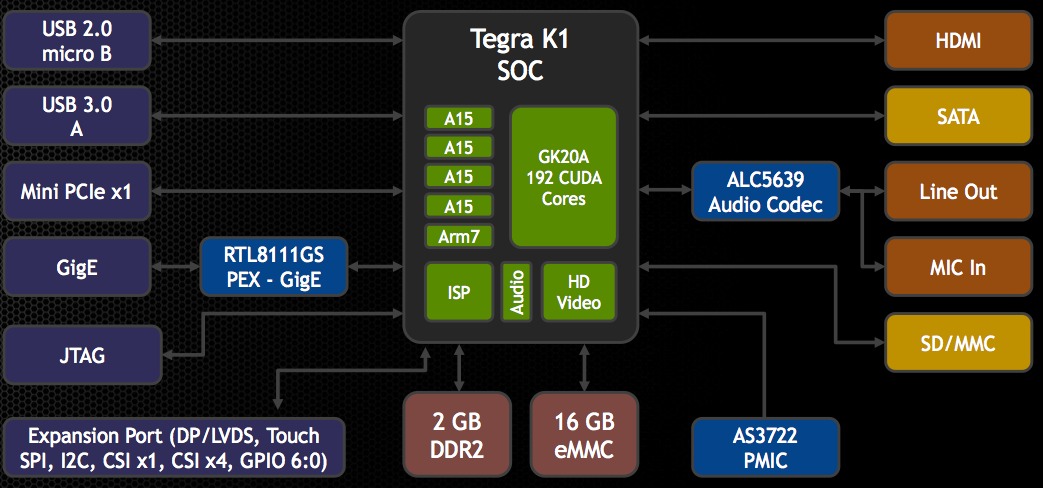
Figure 2. Jetson TK1 provides a robust peripheral suite, along with numerous connectivity options.
Specifically, for computer vision and other camera-based applications, numerous interface options are available for connecting a camera to the board. They include:
- USB3
- GbE
- Mini PCI Express x1, and
- x1 and x4 CSI (camera serial interface) bus options on Jetson TKI's expansion port (whose specifications are already published)
And speaking of vision, it's a key aspect of the software suite that accompanies the Jetson TK1 hardware. As Gary Bradski, President and CEO of the OpenCV Foundation, has discussed in past Embedded Vision Summit and Embedded Vision Alliance Member Meeting presentations, NVIDIA has long supported the development of OpenCV vision processing algorithms optimized for the company's GPUs and other products. NVIDIA's VisionWorks toolkit, according to product manager Jesse Clayton, builds on top of CUDA and conceptually groups together OpenCV-like primitives into higher-level vision and image processing constructs, while still enabling developers to "hook" in support for OpenCV libraries and other software structures. VisionWorks also bundles code examples and documentation.
Additional software included in the Jetson TK1 kit includes the:
- Nsight Eclipse Edition IDE
- NVIDIA Visual Profiler
- Native compiler, debugger, and profiler, and
- Additional CUDA-enabled libraries (cuFFT, cuBLAS, cuSparse, etc.)
And speaking of CUDA, it will remain the exclusive GPGPU (general-purpose computing on graphics processing units) API for Tegra K1 and the Jetson TK1 kit for the foreseeable future, according to Clayton. The alternative industry-standard OpenCL API, he says, is committee-controlled, thereby slowing its evolution in comparison to NVIDIA-controlled (and decade-old) CUDA. Clayton also suggests that OpenCL, intended to be broad enough in scope to encompass support for multiple vendors' products, would be incapable of full optimization for NVIDIA silicon capabilities.
Tegra K1's potential for combining high performance, low power consumption and cost-effectiveness, in general and specifically as implemented in the Jetson TK1 development kit, is notable. Equally notable is NVIDIA's stated embrace of the broader embedded market beyond smartphones and tablets, especially as historical competitors scale back their ARM ambitions. But how (and how well) will the company scale its support offerings to comprehend the needs of a much longer and more diverse list of potential customers? And will the company do an acceptable job of addressing the expanded specification requirements (temperature, voltage, packaging, etc) of these customers' applications, not to mention their lengthier supply sourcing longevity needs? Only time will tell.
Sidebar: A Series of ARM-Based SoCs
Back in October 2011, InsideDSP covered NVIDIA's Tegra 3 SoC. Bucking the trend advocated by CPU core licensor ARM and embraced by other ARM licensees such as Samsung, Tegra 3 did not implement multi-core processor capabilities by combining dissimilar architectures such as the Cortex-A15 (or follow-on Cortex-A12) and Cortex-A7 in a big.LITTLE approach. Instead, in Tegra 3 NVIDIA went with four high-performance Cortex-A9 cores, each of which could be activated and utilized dependent on the system performance needs at any particular point in time. And, in very low performance operating scenarios, Tegra 3 would dynamically switch completely to a single (fifth) Cortex-A9 core optimized for low power consumption.
NVIDIA's follow-on Tegra 4, announced at the January 2013 Consumer Electronics Show, was conceptually similar to the Tegra 3 but migrated all five integrated processor cores from the Cortex-A9 to Cortex-A15s. Tegra 4 also made generational improvements to the integrated GPU core, as well as delivering ISP (image signal processor) and other enhancements. It was followed one month later by Tegra 4i, which back-stepped to the more silicon area-efficient Cortex-A9 and leveraged the freed-up die space (further aided by a Tegra 3-to-4 process transition from 40 nm to 28 nm) to integrate LTE cellular data modem functionality obtained via NVIDIA's mid-2011 acquisition of Icera.
This past January brought another Consumer Electronics Show to Las Vegas and, perhaps not surprisingly, another Tegra arrow to NVIDIA's quiver...two, in fact, both members of the Tegra K1 family. The first, code-named "Logan", is based on the 32-bit ARM Cortex-A15 and is now in production. The other, code-named "Parker", will be derived from a custom NVIDIA-developed 64-bit ARM core called "Denver" and is scheduled to appear before the end of the year. A brief glance at Logan may leave you wondering what all the fuss is about, since like its Tegra 4 predecessor, it's built on a four-plus-one Cortex-A15 CPU core foundation (Figure 3).
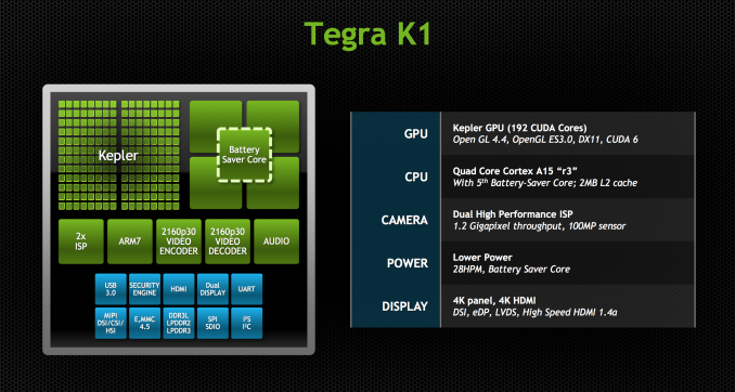
Figure 3. NVIDIA's Logan SoC contains an enhanced version of the ARM Cortex-A15 CPU core previously offered in the Tegra 4, along with integrating a more advanced GPU.
As AnandTech's coverage of the time pointed out, the Cortex-A15 core in Logan is an improved variant of the one previously found in Tegra 4, with enhanced clocked gating and other power efficiency features. And of course, a notable aspect of the 64-bit Parker to come will be its NVIDIA-developed ARMv8 CPU core, enabled by the company's ARM architecture (i.e. instruction set) license and analogous to the design freedom that Qualcomm enjoys with its Krait-based SoCs (Figure 4).
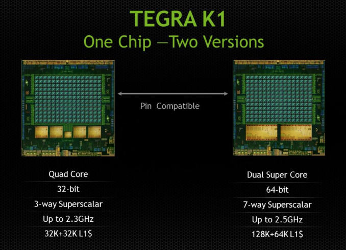
Figure 4. The Parker variant of Tegra K1, to come later this year, will embed a NVIDIA-developed ARMv8 64-bit CPU core code-named Denver.
The other big breakthrough in both Tegra K1 flavors involves the GPU. Historically, the "ULP" GPU cores found in Tegra devices have been architecturally archaic and otherwise dissimilar to those in standalone mobile and desktop GeForce GPUs, as well as to those in the company's legacy nForce core logic chipsets. Beginning with Tegra K1, however, a merging of the mobile and PC graphics roadmaps has occurred. Tegra K1 integrates a Kepler-generation GPU, with Maxwell- and Pascal-based successors already on the future roadmap. This commonality means, among other things, that Tegra K1 is able to leverage NVIDIA's and the broader industry's existing API and application developments around DirectX and OpenGL, as well as CUDA.
The specific Kepler implementation found in Logan comprises a single SMX (streaming multiprocessor) block, encompassed within a single GPC (graphics processing cluster), and including four ROPs (raster operation units) and eight texture units. The GPU's tessellation and geometry units even support both FP64 (64-bit floating point) and FP32 (32-bit) operations. Desktop- and supercomputer-targeted Kepler GPUs run at much higher clock speeds, of course, and contain larger amounts of processing resources. But the architecture commonality between them and the GPU core in Logan is still notable. And the enhanced single-chip integration in this particular Tegra generation offers one other notable benefit; analogous to AMD's Kaveri discussed in last month's InsideDSP, the CPU and GPU cores share access to a common memory space, enhancing overall performance when they're concurrently used in heterogeneous processing applications.
More recently, at March's GTC, company officials made minor tweaks to the future product roadmap, inserting a SoC called "Erista" (based on a Maxwell-generation GPU) in-between Logan and Parker.
Add new comment