
Last month's edition of InsideDSP included the article "NVIDIA and Qualcomm ARM Up Against Competitors," which discussed (among other things) NVIDIA's upcoming five-core Kal-El (i.e. Tegra 3) SoC. Tegra 3 combines four ARM Cortex-A9 cores built out of conventional 40 nm transistors and a fifth Cortex-A9 constructed from low-leakage (albeit switching speed-limited) circuits. The fifth core will operate stand-alone in low-performance usage scenarios (including, ironically, during high definition video playback sessions, thanks to the chip's dedicated-function hardware resources).
When additional processing muscle is necessary, Tegra 3 will speedily (and invisibly, to operating system and application software) transition code execution to the high performance core(s), power-gating the low-leakage Cortex-A9 in the process. Visa versa, when processing demands diminish, control will again return to the low-power core, with the high-performance cores power-gated for minimal overall current draw.
One day after the publication of last month's InsideDSP, we definitively learned (as had been previously rumored) that ASUS' Transformer Prime would be the first Tegra 3-tablet computer to enter production, in December. More recently, rumors have begun swirling regarding the first Tegra 3-based cellular handset, the HTC Edge. And one week after the publication of last month's InsideDSP, we learned about ARM's conventional (i.e. offered to all licensees) alternative to NVIDIA's proprietary heterogenous multiprocessing scheme, as well as hearing the first public details of the "LITTLE" portion of the ARM-branded "big.LITTLE" core mix.
Rarely does a company execute an architectural back-step in rolling out a new product generation, but that's largely what ARM's done with the new Cortex-A7 "Kingfisher" core (Figure 1). Then again, such an approach isn't completely without precedent. Intel, for example, has done it at least twice, with the Pentium M successor (which hearkened back to the Pentium Pro) to the "NetBurst" microarchecture-based Pentium 4, and subsequently with the in-order-only Atom CPU.
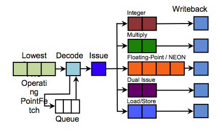
Figure 1. The ARM Cortex-A7 is optimized for low power consumption and silicon utilization.
As with both of those earlier examples, ARM's motivation is two-fold; a reduction in die size coupled with reduced power consumption, albeit with a performance tradeoff. The Cortex-A7 is an in-order, partial dual-issue machine. The dual integer pipelines are eight stages long; the Cortex-A7 combines full ALU (labeled "integer" in Figure 1 above) and partial ALU (labeled "dual-issue") structures, thereby enabling dual-issue instruction execution for some integer operations. Digital signal processing algorithm implementers should note, however, that both conventional multiplication and NEON SIMD operations are single issue-only (the load-store pipeline, as its name implies, handles memory read and write accesses). And all coders should note that the Cortex-A7 does not include the additional transistor- and power-consuming circuitry necessary to handle out-of-order instruction processing. Table 1 below summarizes the high-level feature differences between the Cortex-A7, A8 and A9 core generations:
|
|
Cortex-A7 |
Cortex-A8 |
Cortex-A9 |
|
Instruction decode scheme |
Partial dual-issue |
Dual-issue |
Dual-issue |
|
Integer pipeline depth |
8 stage |
13 stage |
8 stage |
|
Out of order execution support |
No |
No |
Yes |
|
Pipelined floating-point unit |
Yes |
No |
Yes |
|
NEON SIMD support |
Yes |
Yes |
Optional |
Table 1. Comparison of several ARM Cortex-Ax core generations.
While you might think from looking at the table above that the Cortex-A7 would operate at a performance deficit as compared to the Cortex-A8, reality isn't quite as definitive. Note, for example, that the archaic Cortex-A8 architecture is approximately eight years old and has largely been deprecated for new smartphone- and tablet-targeted SoC designs (therefore leading-edge fabrication lithographies). In contrast, the Cortex-A7 contains a more modern branch predictor, further aided by the reduced misprediction penalty of the Cortex-A7's shorter pipeline. Also, the newer CPU core will be fabricated on leading-edge semiconductor processes whose faster switching speeds will compensate (at least in part) for the shorter pipeline depth and the fully synthesized nature of Cortex-A7-based designs versus the more handcrafted Cortex-A8-derived precursors.
The Cortex-A7 instruction pre-fetching scheme has also been improved over the Cortex-A8, and the standard core's L2 cache latency is only 10 cycles, although licensees have the flexibility to alter this parameter in order to optimize die size and other variables. ARM forecasts the Cortex-A7 to achieve 1.5 GHz clock speeds in 28 nm process technologies. The company also believes that each Cortex-A7 core will consume only 1/3 to 1/2 the silicon real estate of the Cortex-A8 alternative; specifically, a 28 nm-fabricated Cortex-A8 will be approximately 0.5 mm2 in size. While ARM envisions entry-level SoCs using the Cortex-A7 exclusively (in either single- or multi-core configurations), higher-end designs will pair one or multiple Cortex-A7s with one or multiple Cortex-A15s in a Tegra 3-like fashion, harnessing the Cortex-A7(s) for low-performance operating situations as a means of extending battery life, while switching to the A15(s) when increased processing muscle is needed.
The Cortex-A15, functional samples of which ARM demonstrated publicly for the first time at the late-October TechCon show, is a high-end triple-issue, out-of-order processor core which also implements virtualization instructions, hardware-accelerated integer division, and 40-bit virtual memory addressing extensions (Figure 2).
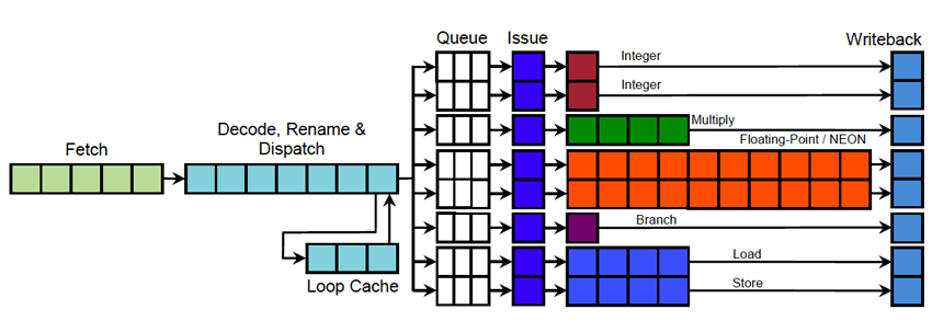
Figure 2. When higher performance is needed, the Cortex-A15 is the preferable core candidate.
Figure 3 shows how ARM envisions Cortex-A7 and Cortex-A15 cores coexisting on a SoC.
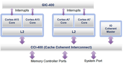
Figure 3. ARM's big.LITTLE scheme balances current draw and processing muscle, courtesy of dynamic core-switching control and power gating capabilities.
Two keys to successful implementation of this vision are the resource-sharing schemes shown above; the GIC (generic interrupt controller) and CCI (cache coherent interconnect). Equally important is the fact that unlike its Cortex-A8 and A9 predecessors, the Cortex-A7 is fully instruction set binary-compatible with its Cortex-A15 "big brother". As with Tegra 3, the dynamic transition between Cortex-A7 and A15 subsystems will be invisible to the operating system and higher-level application software. And, although not strictly required, ARM recommends that on-SoC Cortex-A7 and A15 processing clusters contain the same number of cores.
Speaking of extended memory addressing, while ARM's 40-bit approach announced last year (and implemented for the first time on the upcoming Cortex-A15) enabled the v7 instruction set to access more than 4 GBytes of memory, its multi-stage translation scheme is non-ideal for a number of reasons (performance impacts among them). Therefore, at last month's TechCon, the company also announced the upcoming ARM v8 instruction set, which will be natively 64-bit cognizant. Fully backwards compatible with the 32-bit ARM v7 instruction set, ARM v8 is now available for licensing. The company plans to disclose specific products next year, which it forecasts will appear in prototype systems beginning in 2014.
Combine the above data points with Windows 8's support for both ARM and x86 CPUs, along with the enduring rumors of under-development ARM-based Apple computers, and the next few years should indeed be interesting ones for microprocessor aficionados. Stay tuned for more ARM v8 instruction set news here in InsideDSP as it becomes public.
Add new comment