
Back in October 2011, InsideDSP covered both recently introduced and pending CPU-plus-GPU products from AMD, along with the cores that they were based on. At the time, AMD referred to CPU-plus-GPU integration as "Fusion"; the company has subsequently renamed such products as APUs (Accelerated Processing Units). And back then, AMD was actively selling two APU lines; "Ontario" (along with the higher-power "Zacate" variant), based on the mainstream "Bobcat" CPU core, and the higher-end "Llano", which was derived from the "Stars" CPU core. Stars' lineage traces back to the 2007-era K10 microarchitecture found in the "Barcelona" CPUs for servers and "Phenom" processors for desktops.
AMD's high-end CPU and APU roadmap was ready for a refresh, particularly considering that competitor Intel had begun selling products based on its brand new "Sandy Bridge" microarchitecture. And, as InsideDSP stated 2.5 years ago, the refresh was en route; "Take a look at AMD's published desktop and mobile roadmaps from January, however, and you'll note that Llano has a rather short forecasted lifetime, with 2012 devoted to Bobcat- and Bulldozer-based devices." "Bulldozer", in contrast with the K10 microarchitecture precursor, made a notable architecture shift in striving to free up sufficient silicon room for GPU integration:
Ever since 1989 and Intel's 486DX, which for the first time brought floating-point co-processor capabilities on-board the CPU, a consistent 1:1 ratio between integer and floating point cores had existed across all x86 processor suppliers. Befitting that fact, the "core" atomic unit terminology evolved in short order to encompass the integer-plus-floating point combination. With Bulldozer, AMD takes a fairly radical forward (or, depending on your perspective, backward) step. Each "module" atomic unit contains two integer units bolted to a single 128-bit floating-point core. So keep in mind going forward that when AMD marketing tells you (for example) that the upcoming Opteron 6200 series (code-named "Interlagos") contains up to 16 cores, the reference is to integer cores; the floating-point core count is half that metric.
Since then, AMD indeed rolled out the APUs that it previously forecasted. 2012-era high-end "Trinity" products were based on "Piledriver", a Bulldozer successor that made incremental microarchitecture tweaks; "improvements to branch prediction and FPU/integer scheduling, along with a switch to hard-edge flip-flops to improve power consumption." Roughly six months later, in the first half of 2013, came desktop and mobile variants of "Richland," containing a tweaked Piledriver core that supplied "slightly higher clocks, a software bundle and more sophisticated/aggressive turbo" clocking.
And now, less than a year later, "Kaveri" has arrived. Built on a 28 nm process foundation, versus the 32 nm lithography of Bulldozer- and Piledriver-derived predecessors, Kaveri first and foremost transitions to the "Steamroller" microarchitecture, which aspires to improve on the Piledriver per-thread IPC (instructions per clock) efficiency (Figure 1). Specifically, AMD offers the following Piledriver to Kaveri average improvement estimates for the "fetch" unit:
- Instruction cache misses reduced by 30%
- Mispredicted branches reduced by 20%
- Increase in scheduling efficiency of 5-10%
and the integer scheduler:
- Max-width dispatches per thread increased by more than 25%
along with unquantified "major" improvements in store handling for the L1 data cache.
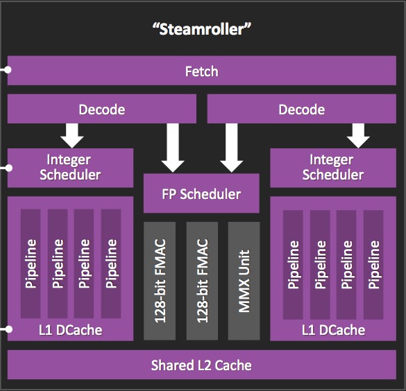
Figure 1. Kaveri's Piledriver CPU core, the third generation of a microarchitecture family that began with 2011's Bulldozer, targets increased IPC (instructions per clock) efficiency.
Kaveri also evolves the on-die graphics core, from "Cayman"-derived graphics (aka the Radeon HD 6900 series, the last of the "Northern Islands" series of graphics cores) in Richland to a successor "Hawaii" (aka Radeon R9) GPU (Figure 2). Kaveri makes evolutionary upgrades to the integrated UVD (Unified Video Decoder) and VCE (Video Coding Engine), with expanded codec capabilities. And this time around, AMD has also integrated the TrueAudio fixed-function accelerator, derived from Tensilica-now-Cadence processor and DSP cores.
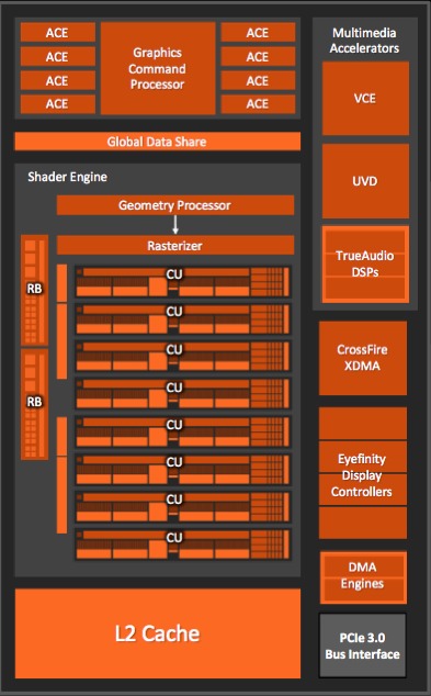
Figure 2. AMD's heterogeneous computing aspirations involve harnessing the integrated GPU on its devices (top), comprised of compute cores (middle) and front-end geometry and back-end render stages (bottom)
If these added and enhanced features were the extent of the Kaveri upgrades, the end result would be a notable update. But Kaveri makes additional improvements, specifically with APU-aware and -appropriate applications in mind, which may not be evident from a cursory review of the die photo (Figure 3). No, your eyes aren't playing tricks on you...the integrated GPU core consumes 47% of the total die area. When AMD acquired ATI Technologies in October 2006, it benefitted in the near term from the incremental revenue and profit garnered from discrete GPU sales.
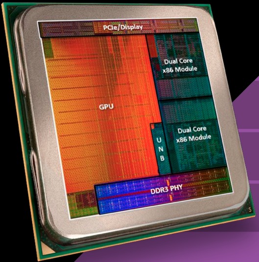
Figure 3. The seriousness with which AMD approaches the APU (accelerated processing unit) market opportunity is evident in the nearly 50% of total Kaveri die area devoted to the graphics processor
However, AMD made it clear from the beginning that the ATI Technologies acquisition was also a long-term play, enabling the company to eventually integrate graphics capabilities alongside the CPU on a single sliver of silicon, and effectively compete against Intel's homegrown graphics cores in the process. Specifically, AMD has long aspired to leverage the GPU's massively parallel (albeit not general-purpose) architecture for more than just graphics processing purposes. AMD has branded the approach with the HSA (heterogeneous system architecture) acronym, and in June 2012 founded an industry consortium to advance the concept in a more industry-encompassing fashion. Notably, AMD has secured the endorsement and participation of ARM and several of its licensees and partners in the HSA Foundation. And equally notably, to date neither Intel nor NVIDIA are foundation members.
Heterogenous computing generally refers to the partitioning of a total processing task among multiple processor cores of different types in a system and/or a SoC within that system, and is enabled by programming languages and APIs such as OpenCL (which does double-duty as a design language). When specifically applied to GPU acceleration of otherwise CPU-executed code, heterogeneous computing is also known as GPGPU i.e. "general-purpose computing on graphics processing units." GPGPU has long been a focus of academic research, along with a few notable commercial successes. As InsideDSP mentioned in October 2011:
Historically, GPGPU has found use in accelerating various still image and video-processing functions, as well as for more specialized applications such as encryption and decryption, virus scanning, and supercomputer database analytics. The migration of the CPU-to-GPU hardware interface beyond predominantly unidirectional PCI to AGP and (especially) PCI Express has been beneficial in this regard, and an on-chip optimized link between the two cores is better yet, at least conceptually. Equally encouraging has been the software API migration beyond vendor-proprietary Stream (AMD) and CUDA (NVIDIA) to industry-standard OpenCL and DirectX Compute.
With Kaveri, AMD believes it finally has an architecture that fully delivers on the APU (i.e. GPGPU) promise, enabling both optimum performance and ease of programming (Figure 4). The company brands the first innovation as "hUMA", for heterogeneous unified memory architecture, i.e. the ability for the GPU and CPU to have equal access to the entire shared memory space, with uniform hardware addressing support and without need for time-consuming CPU<->GPU data shuffles. The second feature addition, "hQ", refers to the claim that the GPU and CPU now have equal flexibility in creating and dispatching work items, with the CPU (for example) no longer needing to go through the latency of high-level graphics driver calls in order to dispatch a job to the GPU. And speaking of high-level graphics driver calls, AMD is also proud to promote Kaveri as the "first OpenCL 2.0-capable chip" (note that the OpenCL v2.0 specification was only recently finalized).
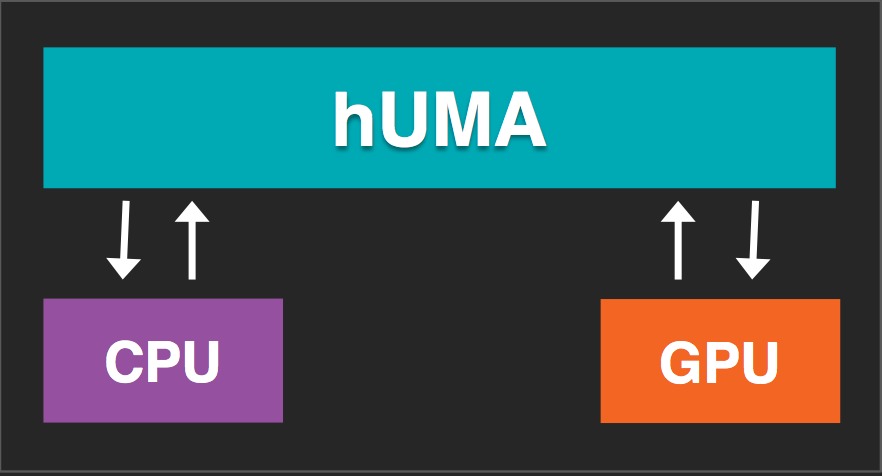
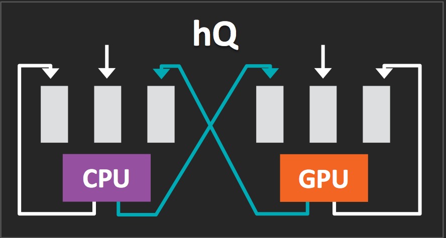
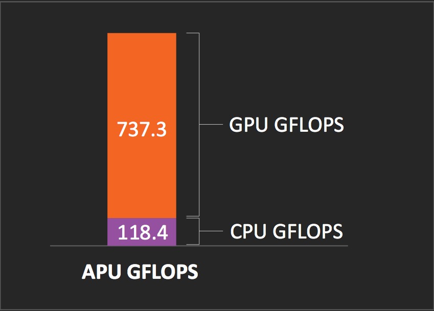
Figure 4. Key to Kaveri's hererogeneous computing capabilities are the unified memory array fully shared between CPU and GPU (top) and the cores' work item creation and dispatch equality (middle), which meld the on-chip processing resources to near-teraflop aggregate peak theoretical performance (bottom)
How well does Kaveri deliver on AMD's promise? Results to date are somewhat inconclusive, judging from published reviews. Keep in mind that so far AMD is only shipping desktop-targeted versions of the APU (Table A). Kaveri may stack up better (both standalone and against Intel competitor devices) in its planned even lower-power mobile variants, which are forecast to operate down to 15W power consumption levels.
|
Model |
A8-7600 |
A8-7600 (same as 45W version) |
A10-7700K |
A10-7850K |
|
CPU modules/integer cores |
2/4 |
2/4 |
2/4 |
2/4 |
|
CPU base max frequency (MHz) |
3,100 |
3,300 |
3,500 |
3,700 |
|
CPU "turbo" max frequency (MHz) |
3,300 |
3,800 |
3,800 |
4,000 |
|
TDP |
45W |
65W |
95W |
95W |
|
L1 cache |
192 KB (I), 64 KB (D) |
192 KB (I), 64 KB (D) |
192 KB (I), 64 KB (D) |
192 KB (I), 64 KB (D) |
|
L2 cache |
2 x 2 MB |
2 x 2 MB |
2 x 2 MB |
2 x 2 MB |
|
GPU cores |
384 |
384 |
384 |
512 |
|
GPU max frequency (MHz) |
720 |
720 |
720 |
720 |
|
Price (unspecified volume) |
$119 |
$119 |
$152 |
$173 |
Table A. Specifications for currently shipping, desktop PC-targeted Kaveri product proliferations
AnandTech's conclusions confirm Steamroller's IPC enhancements over Piledriver, but note that these improvements are counterbalanced by Kaveri's clock speed shortcomings:
In a vacuum where all that's available are other AMD parts, Kaveri and its Steamroller cores actually look pretty good. At identical frequencies there's a healthy increase in IPC, and AMD has worked very hard to move its Bulldozer family down to a substantially lower TDP. While Trinity/Richland were happy shipping at 100W, Kaveri is clearly optimized for a much more modern TDP. Performance gains at lower TDPs (45/65W) are significant. In nearly all of our GPU tests, a 45W Kaveri ends up delivering very similar gaming performance to a 100W Richland. The mainstream desktop market has clearly moved to smaller form factors and it's very important that AMD move there as well. Kaveri does just that.
In the broader sense however, Kaveri doesn't really change the CPU story for AMD. Steamroller comes with a good increase in IPC, but without a corresponding increase in frequency AMD fails to move the single threaded CPU performance needle. To make matters worse, Intel's dual-core Haswell parts are priced very aggressively and actually match Kaveri's CPU clocks. With a substantial advantage in IPC and shipping at similar frequencies, a dual-core Core i3 Haswell will deliver much better CPU performance than even the fastest Kaveri at a lower price.
Kaveri's graphics core more than holds its own competitively, according to AnandTech, at least when used as a GPU:
The story really isn't very different than it was with Trinity and Richland. With Haswell Intel went soft on (socketed) desktop graphics, and Kaveri continues to prey on that weakness. If you are building an entry level desktop PC where gaming is a focus, there really isn't a better option...For casual gaming, AMD is hitting the nail square on the head in its quest for 1080p gaming at 30 frames per second, albeit generally at lower quality settings.
But can the GPU more generally act as a co-processor, counterbalancing any inherent CPU performance shortcoming with its own formidable acceleration potential (and thereby rationalizing the equally formidable silicon area devoted to it)? Here, the operative word unfortunately seems to largely still be "potential":
Kaveri finally delivers on the promise of the ATI acquisition from 2006. AMD has finally put forth a truly integrated APU/SoC, treating both CPU and GPU as first class citizens and allowing developers to harness both processors, cooperatively, to work on solving difficult problems and enabling new experiences. In tests where both the CPU and GPU are used, Kaveri looks great as this is exactly the promise of HSA. The clock starts now. It'll still be a matter of years before we see widespread adoption of heterogeneous programming and software, but we finally have the necessary hardware and priced at below $200. Until then, outside of specific applications and GPU compute workloads, the killer app for Kaveri remains gaming.
As InsideDSP noted nearly 2.5 years ago, software migration beyond vendor-proprietary approaches is a critical factor in encouraging application developers to consider harnessing heterogeneous computing capabilities. Equally critical is a critical mass of sufficient-speed and suffficient-featured GPUs, both integrated and standalone, and from multiple suppliers, with Kaveri's GPGPU implementation arguably the most robust to date.
To that latter point, how successfully can AMD actualize its HSA aspirations without full sanction (including compatible silicon) from Intel and NVIDIA? Only time will tell. Although Marty Johnson, AMD director of product management, admits that competitors' HSA embraces are desirable, they're not essential, as developers have long been used to reluctantly writing code to support multiple standards. Johnson reports that several of the HSA Foundation's implementation specifications are already finalized, with others making steady development progress.
Add new comment