
The effectiveness of a computer vision system is highly dependent not only on the algorithms but also on the quality of the images fed into the algorithms. "Garbage in, garbage out," as the saying goes. More than 20 years of consumer digital camera-fueled image sensor innovations have also delivered cost, resolution, sensitivity, dynamic range, power consumption, and other benefits to visible-light-based computer vision applications. OmniVision Technologies hopes to expand these benefits into emerging NIR (near-infrared) applications with its new Nyxel fabrication process technology, which forms the foundation of the company's new OS05A20 image sensor.
As a recent article published by the Embedded Vision Alliance points out, "computer vision systems aren't necessarily restricted to analyzing the portion of the electromagnetic spectrum that is perceivable by humans. Expanding the analysis range to encompass the IR (infrared) and/or UV (ultraviolet) spectrum, either broadly or selectively and either solely or in conjunction with visible spectrum analysis, can be of great benefit in a range of visual intelligence applications." Security and surveillance systems, biometrics, and ADAS (advanced driver assistance systems) and autonomous vehicles are among the growing list of IR imaging applications. IR light is a dominant percentage of the total (limited) illumination after dark, for example, and can be supplemented by an IR LED illumination source (with the added benefit of not being visible to an intruder). And an IR-based eye scanner, for applications such as retina biometrics and vehicle driver attention monitoring, can operate even if the subject is wearing sunglasses.
The NIR portion of the IR spectrum, beginning at a ~750 nm wavelength and extending to ~1 µm, is largely compatible with conventional silicon-based sensor manufacturing processes and does not require exotic sensor fabrication materials. Silicon-based NIR CCD (charge-coupled device) or CMOS image sensors still usually employ customized designs, encompassing application-tailored pixel geometry and spectrum-tuned microlens arrangements, for example. If they're intended to solely sense NIR light, they may also choose to block visible light from reaching the image sensor by adding low-pass or band-pass filters to the optics or above the sensor. And, as the Embedded Vision Alliance article notes, standard silicon exhibits only limited absorption (typically 10%-25% quantum efficiency, or “QE,” i.e., spectral response) in the NIR range.
That's where OmniVision's Nyxel process enhancement comes in. As explained by Lindsay Grant, the company's Vice President of Process Engineering, in a recent briefing, with a conventional CMOS image sensor process, the majority of NIR photons pass completely through the 1-2 micron thick semiconductor material, versus being captured within it and subsequently measured by each pixel's detector (Figure 1). Single-pixel and small-pixel-count silicon-based NIR detectors get around the issue by employing very deep (50 micron or more) substrate layers, but this approach isn't cost-effective for high-volume applications, nor is it applicable to small-pitch, large-pixel-count image sensor designs.
![]()
![]()
Figure 1. When exposed to NIR illumination, most photons will pass completely through a silicon image sensor that uses a conventional pixel structure (top). Due to the Nyxel approach's slightly thicker trench, in combination with a photon-scattering layer and optical barrier surrounding the trench, more photons are contained within the pixel, therefore detected and measured by it (bottom).
Nyxel also employs a deeper-than-normal per-pixel semiconductor trench, but in this case one only slightly thicker than the norm (the company declined to give dimensions). Instead, OmniVision adds two custom features to the pixel structure (albeit still "easy to manufacture, with comparable yield," according to Grant, although he notes that Nyxel image sensors will still be more expensive than their conventionally manufactured counterparts of equivalent specifications). At the top, just below the microlens, is a "photon absorption scattering" layer which causes photons passing through it to move diagonally rather than remaining in their original vertical paths. An optical barrier lining the sides of each trench also keeps these scattered photons contained to their respective pixels' detectors. The result is a higher percentage of photons remaining within the substrate, and therefore being measured.
Comparative quantum efficiency results measured on two test versions of an OmniVision OV2770 1080p-resolution image sensor with 2.8 micron BSI (back-side illumination) pixel pitch, with one sensor fabricated using a conventional CMOS process and the other leveraging Nyxel enhancements, makes clear the latter's notable QE improvements in the spectrum (Figure 2). Note that NIR light is monochrome, thereby explaining the merging of the red, green and blue curves in the NIR region. Note, too, that the Nyxel-enhanced image sensor also delivers improved QE in the visible spectrum (ranging from ~390 to ~700 nm), especially with red light sources which are spectrum-adjacent to NIR.
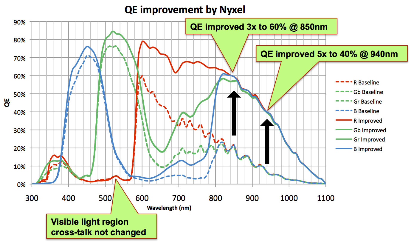
Figure 2. A test image sensor based on OmniVision's OV2770 2 Mpixel device exhibits significantly higher QE in the NIR spectrum range versus its conventional counterpart. It also has higher sensitivity in the visible spectrum, especially with red light sources.
Example image results bear out the laboratory measurements, captured at identical exposure times and again with the two test OV2770 image sensors (Figure 3). Note, for example, the improved sharpness in the OTF (optical transfer function) chart captured using the Nyxel-enhanced image sensor, as well as the ability to read the text in the Nyxel image sensor-captured case.
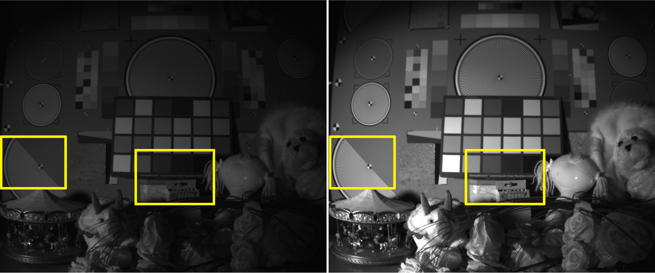
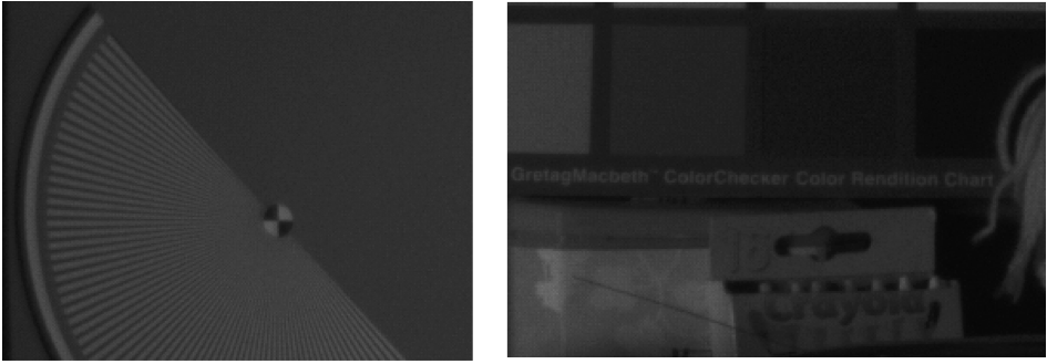
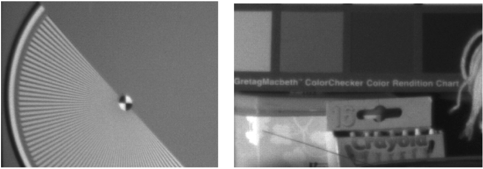
Figure 3. Side-by-side conventional and Nyxel-based sensor image capture results using 850 nm NIR illumination confirm earlier laboratory-measured QE improvements (top). Note in the close-ups how much less distinct the OTF chart and text are with the conventional OV2770 test image sensor (middle) versus with its Nyxel-enhanced counterpart (bottom).
Two weeks after introducing the underlying Nyxel process technology, OmniVision unveiled the first sensor based on it, the 5 Mpixel OS05A20. Leveraging a 2 micron pixel pitch and available in a 1/2.7-inch optical format, the OS05A20 is capable of capturing 2688x1944 video at 60 fps (frames per second), 1080p HD video at 120 fps, and 720p HD video at 180 fps. The OSO5A20 comes in a 6.6 x 5.9 mm CSP (chip scale package) and is now in production; contact the company for pricing.
Add new comment