
Smartphones and tablets may hog the limelight, but advanced driver assistance systems (ADAS) represent another hot technology sector. Market analysis firm Strategy Analytics, for example, expects that by 2021, automotive OEMs will be spending in excess of $25 billion per year on a diversity of assistance and safety solutions (Figure 1). Embedded vision is a critical element of ADAS designs, some of which use vision alone, while others combine vision with radar, LiDAR, infrared, ultrasound, or other sensing technologies.
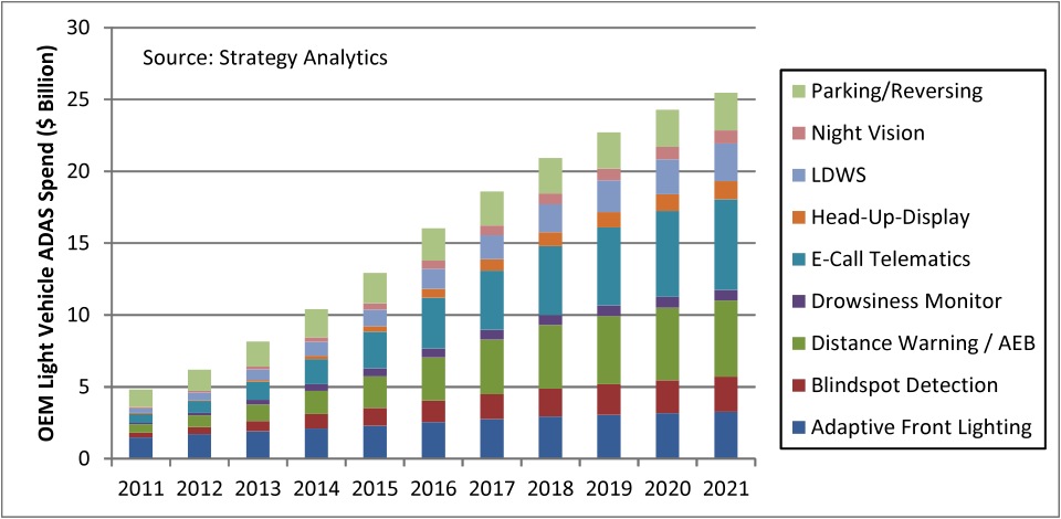
Figure 1. The Advanced Driver Assistance Systems (ADAS) market is expected to grow rapidly in the coming years, delivering a diversity of safety functions.
Two primary factors are key to the continued expansion of the ADAS market: ever-improving solutions for the premium vehicle brands in which ADAS first appeared, and the expansion of ADAS into mass-market vehicles. Two recent announcements from ADAS processor supplier Texas Instruments address both of these market needs (Figure 2).
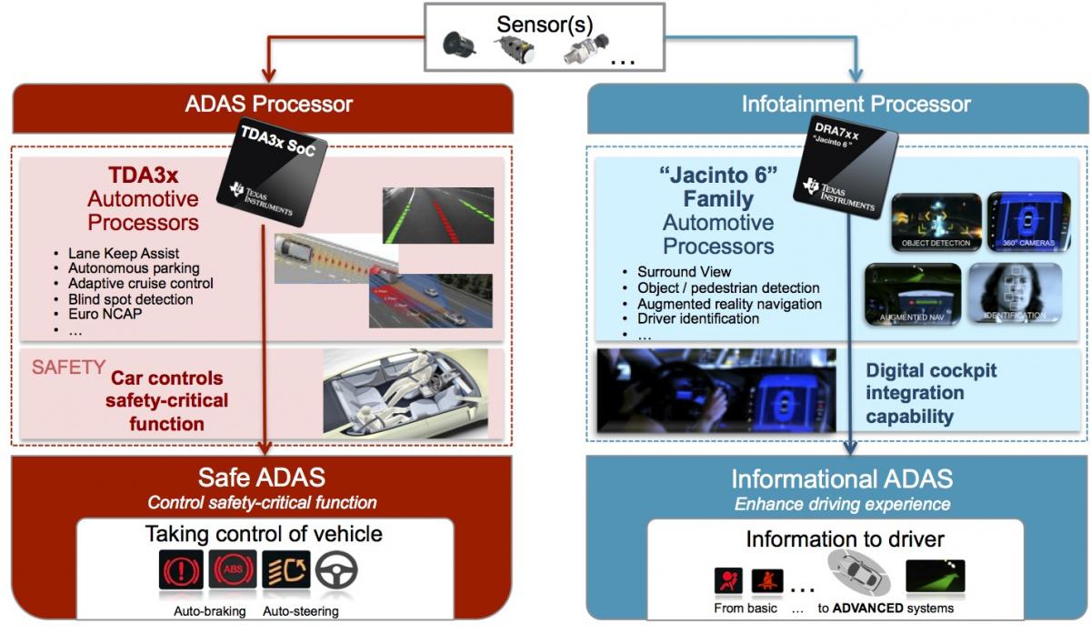
Figure 2. Texas Instruments' TDA3x SoC and latest Jacinto 6 variants both strive to expand the ADAS market, but in different ways.
First is the TDA3x SoC, the follow-on to the TDA2x devices discussed in InsideDSP a bit more than a year ago. Like the TDA2x, the TDA3x is built on a 28 nm process. However, befitting Texas Instruments' aspiration to expand the product family beyond high-end into mid- and even entry-level vehicles, this latest product's feature set has been tweaked (PDF) (Figure 3).
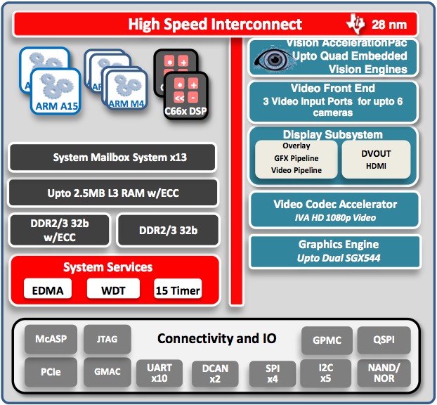
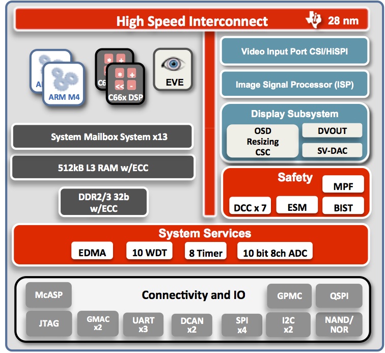
Figure 3. Compared to the TDA2x (top), the TDA3x (bottom) scales down and removes some features, while adding others, striving to simultaneously add capabilities and reduce cost, in order to reach a larger market.
The high-performance dual ARM Cortex-A15 CPU cores found in the TDA2X are not present in the TDA3x; this level of control processing will need to be done elsewhere in the system (such as in the engine control module, i.e. ECM). Similarly, whereas the TDA2x devices contained up to four Embedded Vision Engines (EVEs), each consisting of a 32-bit ARP32 RISC processor core and a 512-bit VCOP vector coprocessor, the TDA3x includes only a single EVE. Instead, you'll find several fixed-function hardware acceleration units (PDF): an image signal processor (ISP), for example, along with a display subsystem (DSS) block.
Whereas the TDA2x family offers up to four ARM Cortex-M4 microcontroller-class cores per chip, the TDA3x family members include two. The TDA3x retains the two C66x DSP cores found in the prior product family. The TDA2x video codec accelerator has been removed in the TDA3x, as has the PowerVR graphics accelerator core; the legacy parallel video input port is only single-lane in this generation. Features added in the TDA3x family include a 10-bit analog-to-digital converter, a standard-definition video digital-to-analog converter, and four lanes of CSI2 or HiSPI video input.
The TDA3x comes in two BGA package options, 15 mm2 and 12 mm2, both with 0.65 mm ball pitch. Both package options are PoP (package on package) in construction, mounting SDRAM on top of the processor. And curiously, although Texas Instruments claims that TDA3x will be more aggressively priced than the predecessor family (without providing pricing specifics), the company also claims that it will implement two notables ADAS features that TDA2x does not: rear camera support, along with radar sensing capabilities. Now sampling, TDA3x will be in production some time next year. Also available is a Vision Software Development Kit (SDK), along with libraries for both EVE and the DSP cores, and the TDA3x SoC Processor Evaluation Module (EVM).
As indicated in Figure 2 above, the TDA3x (like the TDA2x) focuses on “active” safety features, such as automatic braking to avoid collisions, or steering control to keep the vehicle within its lane. Many ADAS systems, however, are purely informational in nature (providing warnings, but not controlling the vehicle), and TI aspires to serve them with upgraded members of the company's Jacinto 6 infotainment SoCs (Figure 4).
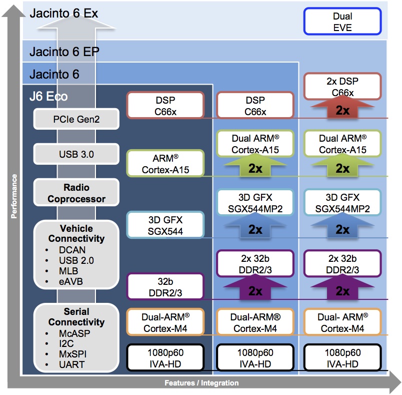
Figure 4. Informational (i.e. warning-only) ADAS facilities are served by two new high-end members of Texas Instruments' Jacinto 6 infotainment processor family.
The initial Jacinto 6 (DRA74x) member of the family was introduced at the January 2013 Consumer Electronics Show, followed by the entry-level Jacinto 6 Eco (DRA72x) in June of this year. New to the product family are two DRA75x devices, Jacinto 6 EP and Ex, providing informational ADAS capabilities in addition to infotainment features. Jacinto 6 EP doubles on-chip C66x DSP facilities offered with Jacinto 6, while Jacinto 6 Ex further expands the chip's vision processing capabilities with the inclusion of dual EVE cores. As InsideDSP noted last year, the 512-bit vector processor integrated in each EVE is capable of up to 16 MACs per cycle (8-bit or 16-bit). And not explicitly shown in Figure 4, but also enhanced in both Jacinto 6 EP and Ex, is the expansion of available USB 3.0 ports from two to three, and Generation-2 PCI Express interfaces from one to two.
Both new Jacinto 6 variants are now sampling to select customers, with production slated for the end of the year. In comparing the Jacinto 6 feature set with that of the TDA3x (Figure 2), you might conclude that the former is the more formidable of the two from a processing resource standpoint. This is true, at least conceptually so; Jacinto 6 includes the dual-core ARM Cortex-A15 removed in the TDA2x-to-TDA3x evolution, for example, along with multiple (optional) EVES and a full-featured graphics core (albeit not an ISP). Keep in mind, though, that Jacinto 6 is intended to simultaneously juggle multiple functions, whereas the TDA3x is an ADAS-focused chip, thereby explaining the latter's active-vs-passive ADAS capabilities.
Add new comment