
Embedded vision, the use of computer vision techniques to extract meaning from visual inputs in embedded systems, mobile devices, PCs and the cloud, is rapidly becoming a significant adopter of digital signal processing technology and techniques. This fact is likely already well known to those of you familiar with the Embedded Vision Alliance, which BDTI founded more than two years ago. If you've visited the Alliance website, you're probably already aware from the content published there that advanced driver assistance systems (ADAS) is one of the fastest growing segments of the embedded vision market. Alternatively, you may be aware of this simply from watching television, since commercials increasingly highlight vehicles' object detection, collision avoidance, lane change control, parking assistance and other ADAS facilities, and not only for high-end models, but also now in mainstream cars and trucks.
Consumers expect more from ADAS as they grow increasingly comfortable with the technology and its capabilities. Commensurate with these expectations, cameras are growing both in resolution and in number. Camera-to-processor connectivity options are also expanding; in some cases--such as LVDS and Flat Panel Display Link (FPD-Link)--the camera transfers uncompressed video, while in others--such as Gigabit Ethernet--the processing intelligence must first decompress the incoming packetized video data. And cameras are also increasingly being supplemented by other sensing technologies, both to expand ADAS capabilities and to enhance the robustness of results (Figure 1). Radar, LIDAR (which employs pulsed laser light instead of microwaves), and ultrasound are some of today's other common options, which increase ADAS systems' success rates and, equally important, minimize the likelihood of an over-aggressive "false positive."
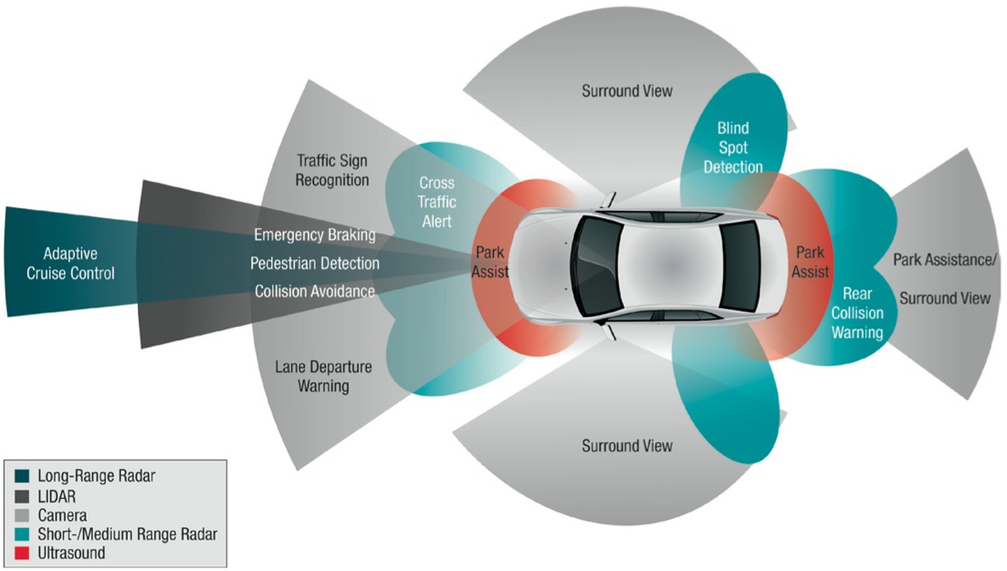
Figure 1. Vision-based analysis is at the core of many ADAS implementations, increasingly supplemented by other sensor technologies to enhance capabilities and increase robustness.
Befitting the burgeoning ADAS opportunity, several IP providers have developed embedded vision-specific processor cores, including CEVA, Tensilica (now part of Cadence) and most recently Apical. Other companies are developing application processors that embed vision processor cores, whether licensed or internally developed; Analog Devices' Blackfin BF60x SoCs with their integrated PVPs (pipelined video processors) are a good example. Still others, such as CogniVue, are perrsuing a dual-prong path, both developing SoCs and licensing their technologies to others. Texas Instruments is the latest supplier to publicly pursue ADAS (the company has quietly been participating in this market for a while) with application-tailored SoC silicon, in the form of the TDA2x family.
TI's new product line divides into three sub-families, the first (TDA2xA) intended for front-view single- or stereo-camera implementations, the second (TDA2xV) tailored for more complex surround (side- and rear-view) camera designs, and the third (TDA2xF) intended for "sensor fusion" processing of data coming from cameras and the other sensor types (such as radar, LIDAR, and ultrasound). The TDA2x superset block diagram reveals the substantial amount of function integration possible courtesy of the SoCs' 28 nm process foundations: one or multiple 750 MHz ARM Cortex-A15 CPU cores, one or multiple 200 MHz ARM Cortex-M4 CPU cores, one or multiple 750 MHz C66x fixed-/floating-point DSP cores, the 532 MHz IVA-HD imaging and video codec accelerator, up to 2.5 MBytes of on-chip L3 RAM with SECDED (single error correct and double error detect) support to address soft error concerns, a PowerVR-based graphics processing core, and a suite of connectivity and other peripherals (Figure 2).
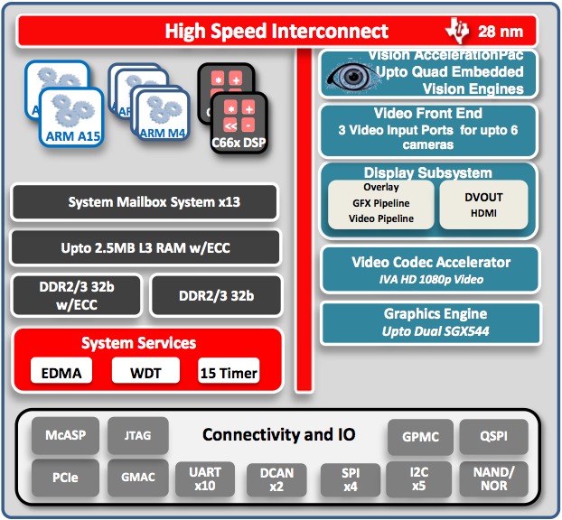
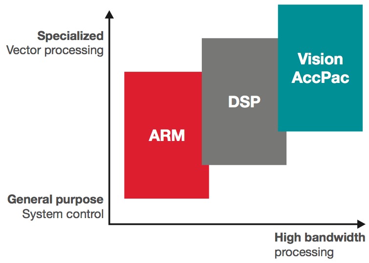
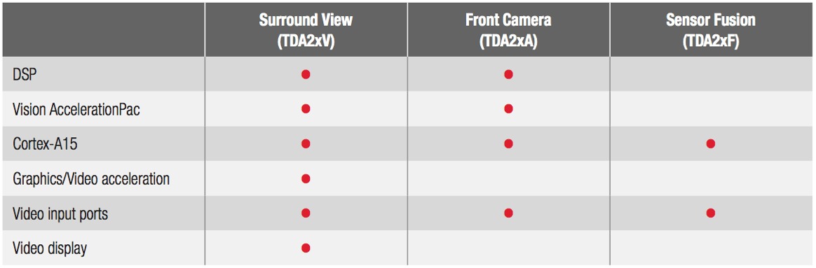
Figure 2. The 28 nm TDA2x SoC family block diagram shows the substantial amount of integration (top), including several different types and amounts of on-chip processing resources (middle). Various family (and sub-family) members leverage this integration potential to varying degrees, addressing specific ADAS implementation needs, along with different cost and power consumption targets (bottom).
Befitting the chips' vision-based ADAS focus, the TDA2xA and TDA2xV product variants also embed the Vision AccelerationPac, a vision-tailored processing core consisting of up to four EVEs (Embedded Vision Engines) (Figure 3). Each EVE comprises a 32-bit ARP32 RISC processor core and a 512-bit VCOP vector coprocessor, the latter running at up to 650 MHz and operating at up to 16 MACs per cycle (8 bit or 16 bit). The resultant vector performance potential is greater than 10.4 GMACs per second per EVE, translating to more than 40 GMACs per second for a chip with four EVE Vision AccelerationPac blocks.
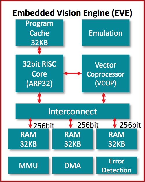
Figure 3. The Vision AccelerationPac found in front- and surround-camera tailored TDA2x SoCs is constructed of up to four EVEs (Embedded Vision Engines), whose combination of RISC CPU, vector coprocessor and local memory can singlehandedly execute many vision processing algorithms, according to TI.
Each EVE's ARP32 RISC processor includes 32 KBytes of program cache, along with a debug module. The VCOP vector coprocessor's dual 8-way SIMD engine provides built-in loop control and address generation. Optimizations in these areas, along with instructions, pipelines and other VCOP attributes, enhance performance and power consumption for the types of data movement, calculation and other pixel operations common in embedded vision algorithms. Speedups of 4x to 12x relative to conventional CPU architectures are common on a diverse range of image processing functions at equivalent power consumption, according to TI (Figure 4). Company officials claim, for example, that each EVE is able to sort an array of 2048 32-bit data points in less than 15.2 μsec. More generally, when running at 500 MHz, each EVE delivers eight-GMAC processing performance and 384 Gbps of data bandwidth, while consuming only 400 mW of power, according to TI.
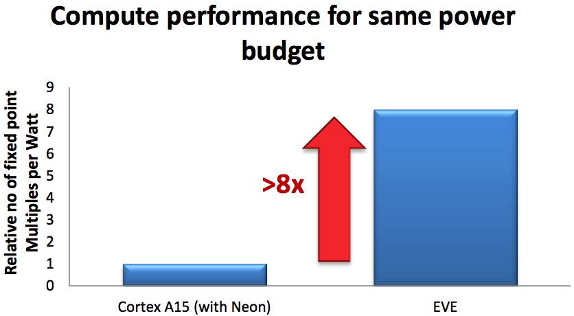
Figure 4. The EVE is feature set-optimized for efficiently running vision algorithms, enabling enhanced energy efficiency compare to running vision code on a host CPU.
Each EVE includes three memory interfaces, each with 256-bit load and store bandwidth to the 96 KBytes of L1 data memory. Each EVE also supports DMA for data transfer to and from the main processor memory, along with an MMU for address translation and memory protection. EVE data memory implements single-bit error detection, with program memory implementing double-bit error detection capabilities. And the DMA engine, ARP32 RISC CPU and VCOP vector coprocessor operate concurrently: the ARP32 can process an interrupt or execute sequential code, for example, while the VCOP executes a loop and decodes another in the background. At the same time, the DMA engine can move data without any processor or memory sub-system stalls. Each EVE also includes built-in support for inter-processor communication via hardware mailboxes.
The Vision AccelerationPac is programmable using TI-developed code-generation tools, which include an optimizing compiler and a simulator integrated into TI's Code Composer Studio IDE. Software can be compiled and run on a PC for simulation, and EVE has built-in support for non-intrusive performance monitoring. The ARP32 RISC core can run full C/C++ programs along with TI's SYS/BIOS RTOS. The VCOP vector coprocessor is programmed with a specialized subset of C/C++ created by TI, called VCOP Kernel C. VCOP Kernel C is a template-based C++ vector library that exposes underlying hardware capabilities through the high-level language. Algorithms written in VCOP Kernel C can be emulated and validated on a PC, using common compilers such as GNU GCC and Microsoft MSVC. Architectural commonality across various TDA2x family members aids in algorithm reuse.
TI currently offers more than 100 programming examples for the Vision AccelerationPac, along with a hardware evaluation module (Figure 5). The existing software library, which the company plans to further expand over time, is primarily focused on algorithm kernels, along with sample data flows. TI also supplies a few prototype applications, primarily for evaluation purposes, but the company does not plan to undertake development of application software for production use. Instead, TI envisions that its customers will do the majority of such programming, among other things reflective of their differentiation desires, and supplemented in some cases by the offerings of TI's third-party development partners.
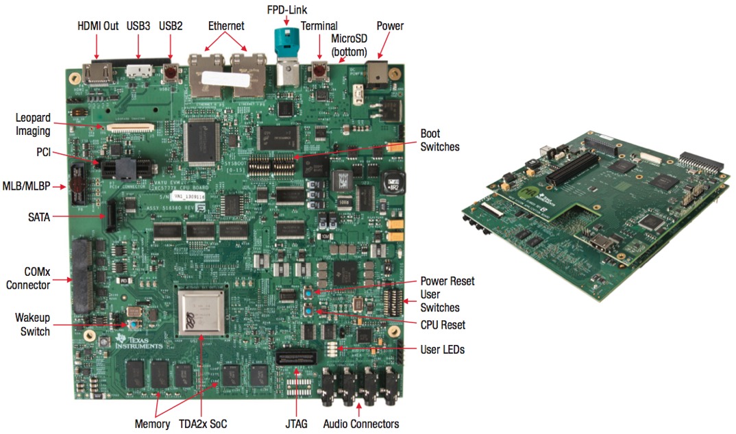
Figure 5. TI's code-generation toolset allows for software simulation and emulation on a PC; an available hardware evaluation module further expands development options.
Initial members of all three TDA2x sub-families are currently sampling, and TI's ADAS Business Manager Brooke Williams reports strong interest and initial design wins for each of them. The company declined to provide either production dates or pricing, however, given that the SoCs are currently intended primarily for a short list of "high-volume automotive manufacturers" with whom TI is already engaged. Longer term, however, TI believes that the chips' feature set implementation is also conceptually appropriate for other embedded vision applications, such as industrial automation, video security monitoring and alert systems, traffic monitoring, and license plate recognition.
Add new comment