
As last summer's formation of the Embedded Vision Alliance suggests, the transition from computer-based intelligent image processing to more compact, cost-effective and energy-efficient embedded vision products is already well underway. CEVA, a company to date best known for its digital signal processing cores found in cellular baseband IC designs, hopes to harness this trend (and, in the process, expand its serviceable market footprint) with the CEVA-MM3101, its latest imaging-tailored offering, which for the first time has been specifically crafted for vision processing applications (Figure 1).
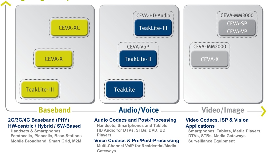
Figure 1. CEVA's historical market presence via DSP cores for cellular baseband functions has more recently expanded into audio and imaging offerings.
As the above graphics notes, the company historically first develops a foundation core architecture (i.e. TeakLite-I, -II and –III, along with CEVA-X and –XC), subsequently creating core proliferations for particular customers and applications. CEVA-MM2000 was derived from the CEVA-X architecture, initially developed for baseband processing applications. CEVA-MM2000 was primarily focused on image encoding and decoding functions, where it handled resolutions up to 720p.
With the CEVA-MM3000, launched several years ago and targeting 1080p at 30fps (as well as 60 fps at some bitrates, color depths and other settings...CEVA claims that the core will even handle QuadHD resolutions in some cases), the company created an application-unique core architecture that combined scalar (CEVA-SP) and vector (CEVA-VP) processors, along with several different on-die memory arrays (Figure 2).
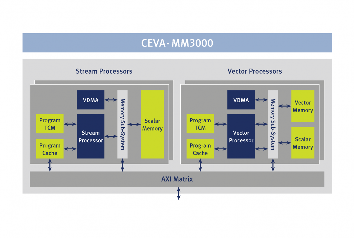
Figure 2. The CEVA-MM3000 combines stream and vector processing within the same core, an architecture framework that's extended by the successor CEVA-MM3101.
Like its MM2000 precursor, the MM3000's focus was on encoding and decoding video and still images. In contraxt, while the CEVA-MM3101 (which the company unveiled last week at the Consumer Electronics Show in Las Vegas) is built on the CEVA-MM3000 framework, its expanded focus encompasses image signal processing and embedded vision functions, along with handling higher pixel counts and frame rates (Figure 3).
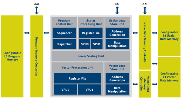
Figure 3. The CEVA-MM3101's combination of application-tailored instructions and integrated memory resources optimizes the performance and power consumption of embedded vision algorithm implementations.
To some degree, these capability enhancements reflect the more advance process lithographies that newer CEVA-MM3101-based SoCs will be built on. According to Eran Briman, CEVA's Vice President of Product Marketing, 28 nm-fabricated CEVA-MM3101 cores will run at approximately 700 MHz and consume less than 0.72 mm2 of silicon area, including 64-96 KBytes of L1 SRAM split between vector, scalar and program memory partitions, plus approximately 128 KBytes of global L2 memory, all of which combine to minimize the need for external memory fetches.
Image signal processing tasks that the CEVA-MM3101 is intended to tackle include:
- Noise removal
- Color correction
- Stabilization
- Selective focus
- Motion blur reduction
- Scaling
- Rotation, and
- De-ringing
And the CEVA-MM3101's targeted embedded vision and scene analysis functions include:
- Object detection
- Face detection and recognition
- Face beautification
- Gesture recognition (reflective of the company's recent investment in fellow Israeli company eyeSight Mobile Technologies)
- Virtual mouse and keyboard
- 3-D map creation, and
- 2-D to 3-D conversion
Focusing first on image processing, which is common to both conventional photography and embedded vision operations, CEVA makes a credible argument that upgradable algorithm implementations (software-based in CEVA's case, versus the hard-wired ASIC "engine" approach) are optimum. Briman pointed out, for example, that processing specifics vary depending on the resolution and pixel pitch of the image sensor in use, as well as being dependent on factors such as the number and location of dead pixels, the noise-versus-ambient light profile of the sensor, and whether or not it incorporates backside illumination. The rapid pace of image sensor technology development makes each of these variables highly unpredictable, as does a customer's desire to source sensors from multiple suppliers for the same system design.
Keep in mind, too, that custom calibration is necessary (or at minimum desirable) for each optics-plus-sensor combination, as well as for each system variant (e.g. for each camera phone model). Now turn your attention to embedded vision, and a flexible algorithm implementation approach is if anything even more credible, considering that at this nascent stage, the techniques for implementing a particular vision processing function are diverse in number. And consider that even in the long term, system-to-system data interchange within the embedded vision ecosystem will be limited. This stands in stark contrast to multimedia capture, editing and playback scenarios, for example, or to wired and wireless networking topologies, all of which demand standardized data formats and interchange protocols by virtue of their interoperability requirements.
Assuming that CEVA is correct in that a software-based algorithm is the optimum implementation approach, which silicon "engine" option should you select to execute the code? Not surprisingly, CEVA recommends the CEVA-MM3101. Briman asserted that his company's new vision processing core consumes 10-20x less power than an ARM Cortex-A9 CPU for the same processing throughput. He also noted that whereas historically at least some degree of image processing capability had been located directly on the CMOS image sensor, alongside the pixel array, the push to higher and higher pixel counts has resulted in processing logic being offloaded to a separate IC (containing, for example, the CEVA-MM3101), with the image sensor's silicon allocation nowadays being exclusively devoted to the image capture function.
With respect to the CEVA-MM3101's architecture optimizations for vision algorithms, the following statement from the company (which I've lightly edited for grammar) may be of interest. "CEVA’s strong experience in video, especially in creating unique encoders, contributes a lot to the support of vision algorithms. Most of these algorithms are based on various motion detections as well as on object and edge detection. The knowledge of our algorithm engineers enabled us to develop specific instructions optimized for video codecs and image signal processing. The CEVA-MM3101 platform was architected through strong cooperation between our algorithm team and architecture team.
"The core's instructions were designed specifically for multimedia support. For example, the SAD (sum of absolute differences) instruction can yield 64 SAD calculations in one cycle. The SAD instruction is used in every motion detection and estimation implementation. Another example is the vector absolute value-subtract-compare instruction, which can calculate eight edge thresholds in one cycle. Edge detection is also frequently found in vision algorithms. The CEVA-MM3101 also has configurable instructions, able to build any filter according to the application and its requirements. Bi-cubic and FIR filters, for example, are commonly used in vision applications."
CEVA supports the CEVA-MM3101 platform with a software development toolkit that includes an optimizing C compiler, IDE, debugger, simulators and a profiler. To aid in vector processor optimization, the IDE provides a view into all core and memory resources. The CEVA-MM3101 toolkit also includes a software suite of video and imaging functions (Figure 4).
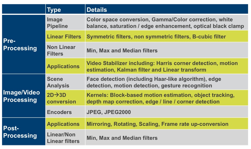
Figure 4. Along with the core and its associated software development tools, CEVA provides a library of video and imaging functions, including image pipeline kernels, linear and non-linear filters, pre and post-processing functions, face detection code, and video codec routines.
The CEVA-MM3101 is currently available for licensing, and the company says that it has already signed a license agreement with an unspecified tier-1 Chinese applications processor developer.
Add new comment