
AImotive has been developing its aiDrive software suite for advanced driver assistance systems (ADAS) and autonomous vehicles for nearly a decade. As the computing demands of its algorithms continue to increase, the company is finding that conventional processor approaches aren't keeping pace. In response, and with an eye both on vehicle autonomy and other deep learning opportunities, the company began developing its own inference acceleration engine, aiWare, at the beginning of last year. An FPGA-based evaluation kit for the IP is now available, with an initial ASIC implementation scheduled to follow it to market early next year.
Originally a side project of parent company Kishonti, a compute and graphics benchmarking technologies provider, AImotive (originally known as AdasWorks) became a standalone entity in mid-2015. NVIDIA has been a notable hardware partner for aiDrive development and demonstrations, although AImotive's head of hardware Marton Feher and head of European sales Bence Varga both emphasized in a recent briefing that the company also works with a number of other silicon suppliers representing multiple processor architecture types: CPUs, GPUs, FPGAs, DSPs, etc.
Feher and Varga also stressed that the company's historical processor partnerships would remain key going forward, particularly with respect to the acceleration of deep learning model training. For inference, however, when a neural network analyzes new data it’s presented with based on its previous training, processors are increasingly being challenged by the combination of:
- Higher camera resolutions and frame rates
- An increasing number of cameras per vehicle
- Increasingly complex algorithms employed to analyze and respond to those cameras' captured images
- Increasingly common merging of images with other sensor data (radar, LiDAR, ultrasound, GPS, etc.), and
- The need for real-time response to changing driver, vehicle and environment factors.
As the performance demands of deep learning algorithms have grown, the limitations of legacy processors have become increasingly apparent, according to Feher and Varga. Some legacy processors, for example, were initially targeted at graphics or other functions and are therefore non-optimal for deep learning inference. Specifically, a 32-bit floating-point architecture is overkill from both silicon area and power consumption standpoints, in their opinion, when used for algorithms in which 8-bit integer operations are sufficient. Memory latency, too, is often an issue; a MAC-rich architecture capable of running at high clock speeds may significantly underperform its potential if it's frequently forced to wait for external DRAM accesses to complete.
Consider, for example, a simple neural network that performs classification of 224x224 pixel source images (Figure 1). Even with the use of 32-bit floating-point operations, the layer inputs and outputs (along with weights) can likely fit fully into on-chip memory.
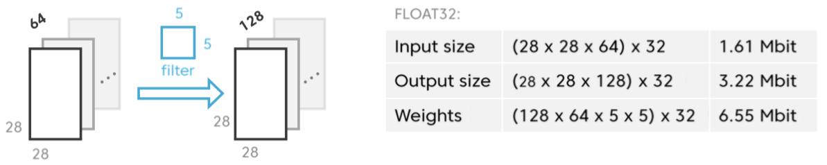
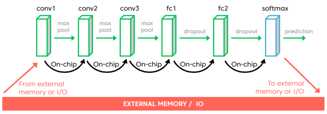
Figure 1. Neural networks that process small input images, contain few hidden layers and implement relatively simple functions may benchmark well (top) because they fit in on-chip memory (bottom) but are increasingly unreflective of real-life implementations, according to AImotive.
With a more complex neural network (deeper in terms of layer count, with a larger number of layer input/output channels, etc.) and/or with larger source image sizes, however, the necessity of relying on external memory becomes increasingly likely. Consider, for example, a segmentation and boundary boxing application that operates on 1080p (1920x1080 pixel) image inputs (Figure 2). In such a case, there's no way to transition data from one hidden layer to another without use of external DRAM, even if you quantize from a 32-bit floating point to 8-bit integer format. And while tiling (dividing each network layer input into smaller-sized tiles for sequential processing) would in theory allow for the use of on-chip memory, in practice the diversity of layer input and filter window sizes that an accelerator would be tasked with comprehending across multiple applications, customers and implementations would likely still result in size mismatches that would compel the use of external DRAM as a buffer to store intermediate results.
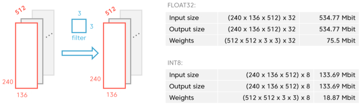
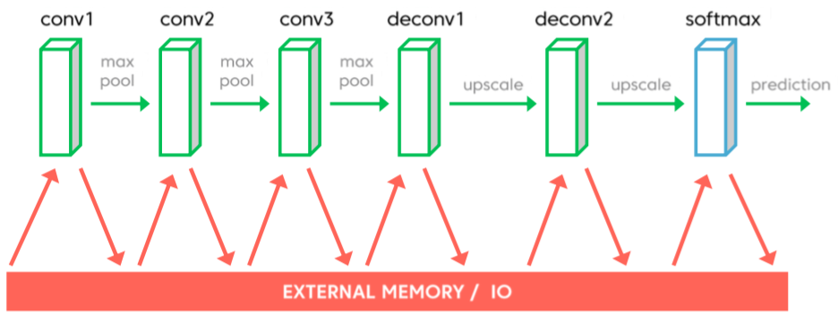
Figure 2. Larger source images and deeper neural network hidden-layer topologies (top), in combination with traditional processing architectures, necessitate the use of slow, power-hungry external memory (bottom).
Feher offered several guiding principles that shaped aiWare's development:
- Read all input data from, and write all output data to, external memory as few times as possible: preferably only once.
- Keep the amount of intermediate results to a minimum.
- Use INT8 instead of either FLOAT32 or FLOAT 16 (to reduce both the computation workload and memory footprint), while minimizing the resultant impact on algorithm accuracy.
- Maximize MAC utilization.
- Minimize on-chip routing buffering.
Feher also explained that AImotive's dedicated-function approach was intended to accelerate between 96-100% of the operations commonly used in deep learning inference. Any remaining, rarely found inference tasks would be wasteful to implement in aiWare after considering the required incremental silicon area, power consumption, and design complexity, he opined; they could alternatively be handled in a hosted general-purpose DSP or other processor core. Conversely, he believes, deep learning training involves a huge variety of operations, which frequently differ across varying neural network architectures, methodologies and intended tasks. Such training functions wouldn't be a good candidate for fully dedicated hardware acceleration, unless perhaps a supplier attempted to only support one framework.
aiWare's LAMs (Layer Acceleration Modules) are the core's compute nexus (Figure 3). Since the architecture is implemented in "soft" RTL versus "hard" IP, a licensee can customize the LAMs to fit particular needs. 8x8 multipliers might dominate a convolution-centric implementation, for example, whereas a LAM tailored for max pooling functions would also include a significant number of comparators. The target clock speed, even on the 16 nm processes that AImotive believes will service initial licensees' production needs, are modest: in the range of 500 MHz, reflective of the architecture's massive parallelism and hoped-for high utilization efficiency. And keeping clocks low also keeps power consumption low; AImotive's target on this same process lithography is less than 2W/TMAC/sec.
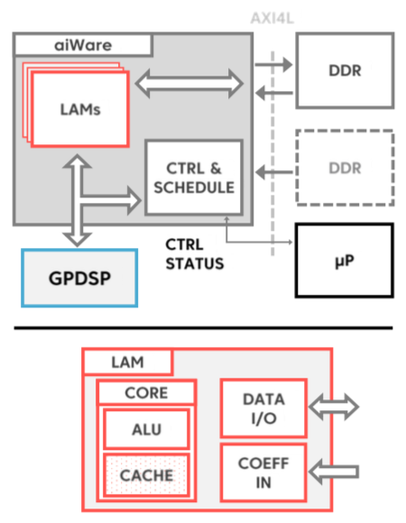
Figure 3. 8-bit quantization is an essential element of the aiWare architecture.
Conceptually, at least, AImotive's approach with aiWare is reminiscent of Google's TPU (Tensorflow Processing Unit), which similarly focuses on inference acceleration and whose first-generation architecture details the company revealed in May (shortly before launching its second-generation devices). In Google's case, of course, the inference is being done on a server, a much different environment than the "black box" of an automobile, for example. And whereas Google's TPUs are full-chip (and reportedly quite large, at that), aiWare is intended to be an embedded core within a larger SoC.
Speaking of chips, AImotive and partner VeriSilicon are in the process of designing a 22 nm FD-SOI test chip, which is forecast to come out of GlobalFoundries' fab in Q1 2018 (Figure 4). It will feature a 1 TMAC/sec aiWare core, consuming approximately 25 mm2 of silicon area; a Vivante VIP8000-derivative processor core will inhabit the other half of the die, and between 2-4 GBytes of DDR4 SDRAM will also be included in the multi-die package. The convolution-tailored LAM in this test chip, according to Feher, will have the following specifications (based on preliminary synthesis results):
- 2,048 8x8 MACs
- Logic area (including input/output buffering logic, LAM control and MACs): 3.45mm2
- Memory (on-chip buffer): in the range of 5-25mm2 depending on configuration (10-50 Mbits).
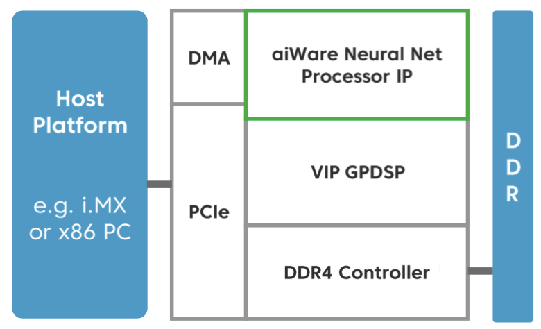
Figure 4. An under-development test chip mates a 2,048-MAC aiWare acceleration core and a VeriSilicon Vivante processor core, along with other interface function blocks.
In advance of test chip availability, AImotive has developed an evaluation kit that implements an aiWare core on a FPGA development board, as a PC add-in card form factor. The kit includes an aiWare binary image, an x86 driver for Linux, a preliminary version of the SDK along with a Caffe plugin (which, according to Feher, allows for efficient floating point-to-INT8 conversion), and various neural network and API usage examples. The company's intention with the evaluation kit is threefold regarding potential licencees' capabilities:
- Evaluate and benchmark the aiWare IP with AImotive's example neural network
- Feed custom videos as input and receive segmentation output
- Run licensees' own networks/layers and benchmark speed, latency, etc.
Characteristics of the aiWare core in the evaluation kit are as follows:
- 1,024 MACs
- 22 Mbit BRAM (block RAM)
- Intel/Altera Arria 10 GT1150 FPGA
- LUT utilization: 66%
Khronos' under-development NNEF (Neural Network Exchange Format) is, according to Feher, a key component in the company's hoped-for success with aiWare (Figure 5). The standard encapsulates neural network structures, data formats, common operations (convolution, pooling, normalization, etc.) and formal semantics; its intent is to allow for robust interchange between various frameworks, inference engines, and other toolkits, thereby (as with a graphics API, for example) abstracting any particular hardware implementation. AImotive is currently leading the NNEF working group.
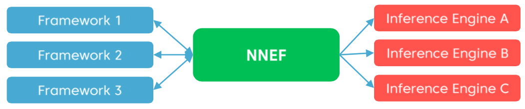
Figure 5. Khronos' NNEF standard, by abstracting deep learning frameworks and hardware implementations of them, enables new processing architectures such as aiWare to more easily enter established markets.
Regarding the company's SDK plans, Feher had the following comments: "The lack of proper software support for any hardware will turn developers and customers away. We understand this challenge and have been developing our software tools in-house to support developers on every level, from beginner to expert. Our SDK is separated into online and offline components, to support embedded and real-time/safety critical systems. We ensure this by keeping the online/real-time portion of the SDK lightweight, basically handling only the high-performance, low-latency execution of data generated by the more complex offline module."
"The offline module handles NNEF parsing and incorporates a custom aiWare C/C++ building API. By default, the offline portion of the SDK exports the binary network information and weights into a deployable file, which is then used by the online portion of the SDK. This approach helps to ensure that the system is safety critical-certifiable. We have also included a clever interconnection system that can interface directly with the execution engine of the online module to enable fast prototyping and testing. The SDK is not yet complete, but basic versions of these functions are already available and bundled in the FPGA evaluation kit."
AImotive's aiWare is only the latest example of the burgeoning list of deep learning processor architecture and supplier options available to developers. Not all of them will likely remain on the list long-term, in this latest example of the tech industry's longstanding "survival of the fittest" Darwinist evolutionary-culling tendencies. But regardless of whether or not a particular candidate outlives its competitors, the ideas behind (and concepts within) its implementations will still likely advance the deep learning industry in a broader sense.
For more information on AImotive, see the company's recent demonstrations at the January 2017 Consumer Electronics Show:
and the May 2017 Embedded Vision Summit:
Add new comment