
Qualcomm formally unveiled the Snapdragon 835, its latest premium-tier mobile processor, at the Consumer Electronics Show earlier this month after a last-fall "tease". Sporting eight CPU cores and fabricated in Samsung’s latest 10 nm process, the new chip represents the next step in the evolution of the Snapdragon 800 product line, building on features previously introduced in the Snapdragon 820 and 821.
The 14 nm-fabricated Snapdragon 820, initially unveiled in March 2015 with fuller disclosure by the end of that same year, had marked the first use of the company's 64-bit Kryo custom ARM processor core—four of them, actually, two in a (high) performance cluster and two others in a (low) power cluster, alternately enabled as system resource needs dictated. Of particular interest to InsideDSP's digital signal processing audience, the Hexagon "compute" DSP core used for computer vision and various multimedia functions (one of three total Hexagon DSPs on the SoC, the others for sensor fusion and cellular communications tasks) was significantly advanced with respect to its support for vector extensions and other enhancements.
Last summer's Snapdragon 821, also fabricated on Samsung's second-generation 14nm FinFET process, delivered modest clock speed improvement for various core subsystems; the two-core Kryo CPU performance cluster went from 2.15 GHz to 2.34 GHz, for example, with the CPU power cluster boosted from 1.59 GHz to 2.19 GHz and the Adreno 530 GPU moved from 624 MHz to 653 MHz (Table 1).
|
SoC |
Snapdragon 835 |
Snapdragon 821 |
Snapdragon 820 |
|
CPU |
4x 2.45 GHz Kryo 280 (Performance) 4x 1.9 GHz Kryo 280 (Power) |
2x 2.34 GHz Kryo (Performance) 2x 2.19 GHz Kryo (Power) |
2x 2.15 GHz Kryo (Performance) 2x 1.59 GHz Kryo (Power) |
|
GPU |
Adreno 540 |
653 MHz Adreno 530 |
624 MHz Adreno 530 |
|
"Compute" DSP |
Hexagon 862 |
Hexagon 860 |
Hexagon 860 |
|
ISP |
Spectra 180 1x 32Mpixel or 2x 16Mpixel |
Spectra 1x 25Mpixel or 2x 13 Mpixel |
Spectra 1x 25Mpixel or 2x 13 Mpixel |
|
Modem |
X16 LTE |
X16 LTE |
X16 LTE |
|
Process Node |
Samsung 10nm LPE (1st gen) |
Samsung 14nm LPP (2nd gen) |
Samsung 14nm LPP (2nd gen) |
Table 1. Snapdragon comparative specifications.
With the new Snapdragon 835, Qualcomm migrates the architecture to Samsung's newest 10nm FinFET process; the company has particularly focused the latest chip's nearly 3 billion transistors at the CPU clusters and cache. Now, instead of four total CPU cores, you'll find eight; four each in the performance (2.45 GHz peak) and power (1.9 GHz max) clusters. L2 cache sizes have doubled to 1 MByte (performance) and 2 MByte (power). Qualcomm also explicitly refers to them as "Kryo 280" cores, this time around, versus a generic "Kryo" designation in the Snapdragon 820 and 821 (Figure 1). According to the company's technical marketing communications manager, Francisco Cheng, the "2" refers to a second-generation Kryo design, whereas "8" is a family member designation within that generation. Similarly, the previous "Spectra" ISP is now explicitly referred to as the "Spectra 180".
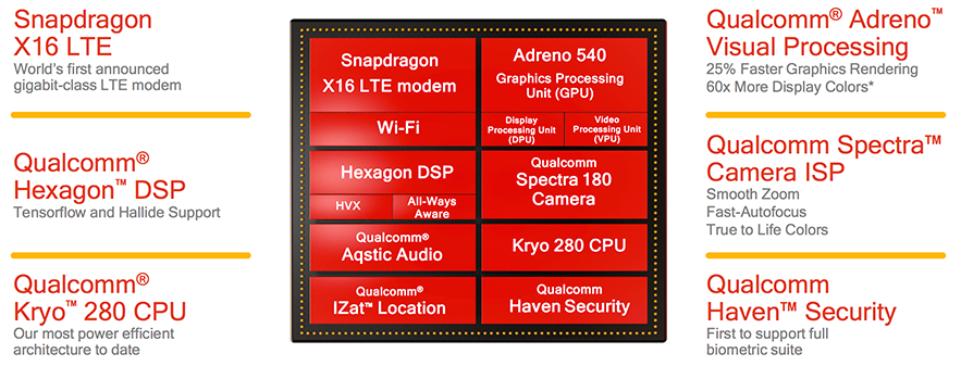
Figure 1. Whereas each Snapdragon 835 processing core subsystem received only modest upgrades, the sum of the constituent parts (thanks, too, to a substantially higher transistor budget) is more significant.
Other core subsystems that previously had explicit monikers have been only slightly incremented this time around; the Adreno GPU from 530 to 540, and the Hexagon DSP from 860 to 862. Cheng and his Qualcomm peers who participated in a recent product briefing were loath to discuss architectural enhancement details related to any of the core subsystems, preferring to speak only in terms of resulting benefits. The Spectra 180 ISP now supports up to a single 32 Mpixel image sensor, or alternatively a dual 16 Mpixel-maximum sensor array, whereas the prior Spectra ISP handled up to a single 25 Mpixel image sensor or dual 13 Mpixel-maximum sensor array. The Adreno 540 GPU is claimed to be "25% faster" than the Adreno 530, but the usage conditions under which this comparison was measured are not public.
The Hexagon 862 DSP core similarly represents a relatively modest evolution beyond its Hexagon 860 precursor, specifically in the areas of added instructions for deep learning and other "compute" operations. As with the Snapdragon 820 and 821, the Snapdragon 835 supports the company's Neural Processing Engine (NPE) SDK announced at last May's Embedded Vision Summit, and Qualcomm has worked closely with Google to optimize both silicon and associated software for the TensorFlow deep learning framework. The fruits of their shared labor are documented in a recent Qualcomm-published blog post and associated demonstration video. In other Hexagon-related news, albeit in this case with a communications flavor, the integrated cellular modem now supports Category 16 1 Gbps (versus previous Category 12 600 Mbps) LTE peak download speeds. And as for the Kryo CPU enhancements, they seem to be more than just clock speed boost-related, since the Snapdragon 835 is the first ARM-based SoC that Microsoft has sanctioned to run Windows 10 32-bit x86 binaries in emulation mode.
Bigger picture, the comparative power consumption and die size metrics between the Snapdragon 835 and Snapdragon 821 predecessor are also somewhat unclear. Qualcomm claims approximately 25% lower power consumption for the Snapdragon 835, but again won't comment on the usage scenario with which this comparison to the Snapdragon 821 was determined. Although the 35% reduction in package area is impressive, the company won't provide similar statistics for the area reduction of the die inside the package (Figure 2). Pragmatically, however, given the doubling up of both CPU core count and L2 cache sizes, any die size reduction delivered by the 14 nm to 10 nm process node migration is notable.
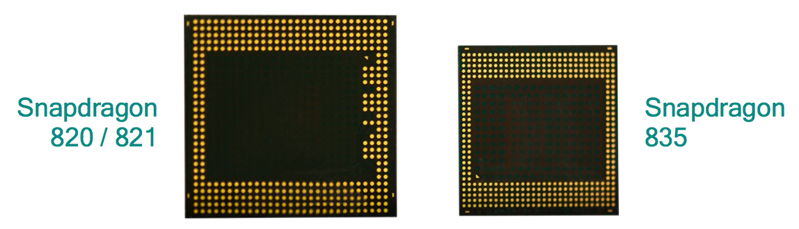
Figure 2. Qualcomm is proud to tout its 35% package size reduction, but mum on the comparative die sizes inside each of them.
The Snapdragon 835 has been production-ready since last fall, and the first smartphones and tablets based on it are expected later in the first half of this year; the February 27-March 2 Mobile World Congress conference is a safe bet for announcements. And smart glasses manufacturer ODG has already announced a Snapdragon 835-based product at the Consumer Electronics Show earlier this month. Two years ago, Qualcomm's first 64-bit SoC, the Snapdragon 810 based on conventional ARM Cortex CPU cores, stumbled out of the block due to its poor power consumption characteristics. Since then, the company has impressively regained its stride, both by getting its heat problems under control and by transitioning to its own 64-bit CPU architecture. The Snapdragon 835 represents a promising next step in evolution for this product family—but we'll have to wait for products based on the 835 before we can understand its performance in real-world use cases.
Add new comment