
The general trend of recent times is toward developing DSPs that are specialized for particular "killer" applications, such as wireless or embedded vision. Many other applications also need DSPs, however, and Cadence's Tensilica Fusion DSP core family, which complements the company's more application-specific DSPs, is one example of an architecture that aspires to serve a broader range of general applications. When Cadence introduced the first Fusion family member (now referred to as the Fusion F1) in April 2015, the core targeted applications with relatively modest performance needs, such as wearables and IoT devices.
This time around, with the newly released Tensilica Fusion G3, the company is targeting higher-end markets such as automotive, consumer, and industrial, and the architecture's been beefed up to match (Figure 1). The number of available VLIW issue slots has doubled, for example, to four. Whereas the base Fusion F1 configuration included only a single 32x32 MAC (multiply-accumulate unit), with an optional upgrade adding four more 16x16 MACs, Fusion G3 comes standard with four 32x32 fixed-point MACs, capable of supporting a range of integer arithmetic operations from two 64x64 MACs/cycle to sixteen 8x8 MACs/cycle, along with four single-precision 32-bit floating point FMA (fused multiply add)/MAC units. And whereas the vector FPU (floating-point unit) remains an optional upgrade, in Fusion G3 it now handles both single- and double-precision arithmetic, versus the single precision-only FPU option in Fusion F1.
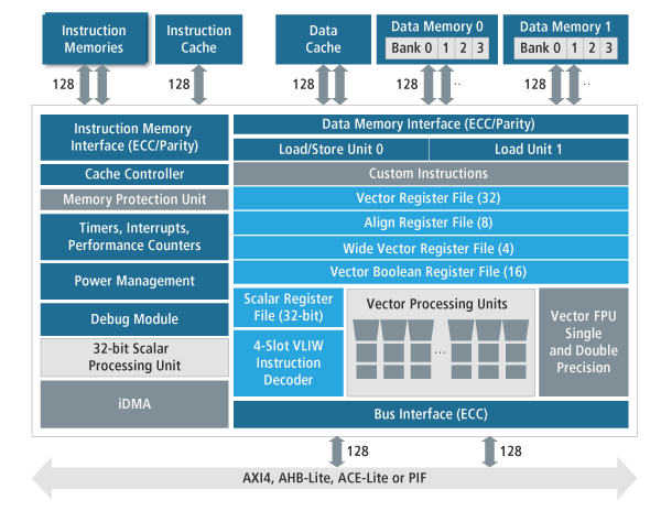
Figure 1. Cadence's Tensilica Fusion G3 DSP core makes significant upgrades to the arithmetic capabilities of its Fusion F1 precursor, befitting its focus on higher-end applications.
The Fusion G3 core, according to Paul Garden, Product Marketing Director for Tensilica IP, and Amir Kamalizad, Senior Technical Manager for Tensilica IP, is capable of running at up to 750 MHz on a 28 nm process, increasing to 1 GHz on a 16 nm process. By fully utilizing all four available VLIW slots in conjunction with the 32-bit FMA/MAC units and the vector FPU, the core can calculate up to 16 single-precision FLOPS per cycle, translating to peak 32-bit floating-point throughput at 1 GHz of 16 GFLOPS. Befitting the higher-end application focus, Fusion G3 also includes optional ECC/parity support for instruction fetches, one of the upgrades found in the overall improved memory controller, which also implements discrete instruction and data buses for both main memory and cache accesses. Additional (and, as with the FPU and ECC/parity units, optional) memory access-related enhancements come from the memory protection unit and DMA controller, both shown in the above block diagram.
At this early stage in the architecture's life cycle, Garden and Kamalizad were unwilling to share either silicon area or power consumption estimates. For these and other non-public specifications, you'll need to talk to Cadence directly (and likely sign a NDA). Speaking of product maturity, Cadence reports that its lead Fusion G3 customer has already taped out first silicon of a SoC containing the core; general licensing availability is slated for October of this year. Fusion G3 support is already in place within Cadence's Xtensa Xplorer toolset, which includes an auto-vectorizing C/C++ compiler, along with a 550+ function DSP software library. On that note, keep in mind that whereas both Fusion F1 and Fusion G3 are built on a common Tensilica Xtensa LX7 CPU core foundation, their DSP subsystems are dissimilar, translating to a dearth of DSP object code compatibility between them.
For more on Cadence's Tensilica Fusion G3 DSP core, see the following "Whiteboard Wednesdays" introduction video presented by Product Marketing Director Paul Garden (Video 1):
Video 1. Cadence's Paul Garden introduces the Tensilica Fusion G3 DSP core.
Add new comment