
Instruction set flexibility can go a long way toward extending the usable life of a processor architecture. Sooner or later, however, instruction set enhancements to an existing architecture foundation run out of steam, and a more fundamental evolution is necessary. This explains why Cadence Fellow (and former Tensilica co-founder and CTO...Cadence announced in March that it was acquiring Tensilica) Chris Rowen took to the stage in mid-October to unveil the company's latest tenth-generation Xtensa CPU architecture, along with the fifth-generation Xtensa LX, which adds VLIW and other advanced capabilities (Figure 1).
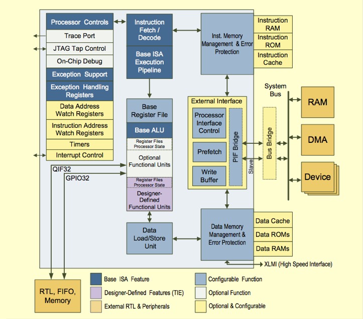
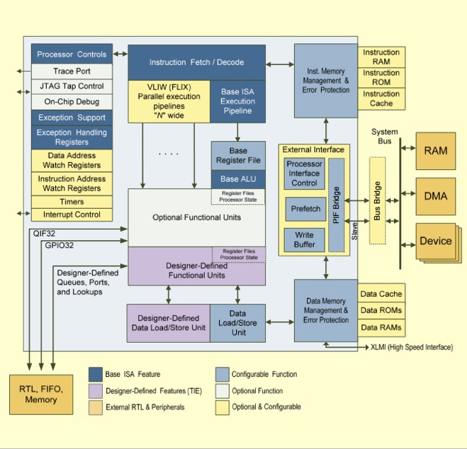
Figure 1. Cadence's Xtensa 10 (top) and Xtensa LX5 (bottom) represent the company's most extensive processor core evolutions since the beginning of the decade.
Rowen began his talk by positing, "If you were an application, what would you dream?" His answer focused on three fundamental development areas: memory subsystem improvements to boost performance, optimizations to reduce power consumption, and debugging-related ease-of-use enhancements (Figure 2).
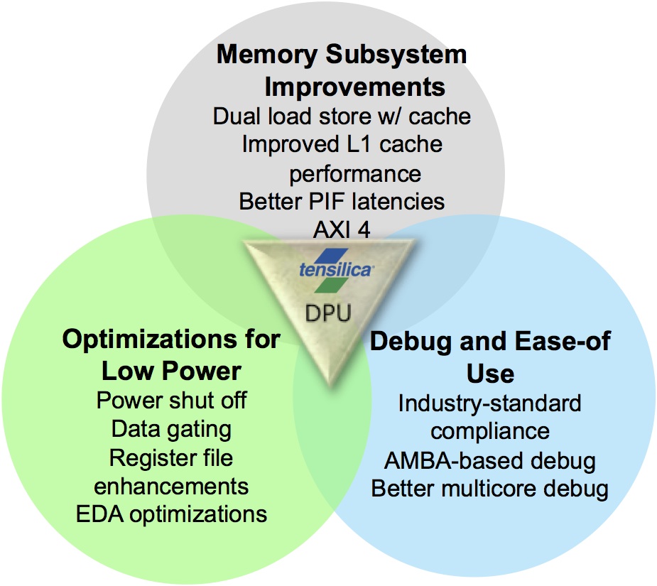
Figure 2. Power efficiency, memory bandwidth and time-to-market were the three key areas of attention in these particular architecture iterations.
Cadence includes multiple power domains on the Xtensa 10 and LX5, each operating at a common voltage and handled by an on-chip power management control block for reduced leakage current. Dynamic power consumption also receives focus; it's possible, for example, to "gate" semantic combinational logic via a one-hot select signal. In combination with memory data "gating" support, Cadence estimates 2 - 8% in dynamic power savings just due to these two added capabilities.
Power consumption optimization is also addressed in the memory system by the up-to-256-byte loop buffer, a set of registers intended to hold small code segments that are executed repeatedly. 256 bytes may not seem like much memory at first glance, but Cadence claims that its reference MP3 decode algorithm, for example, spends 40% of its cycles completely within the loop buffer. And by executing this and similar loops out of the "L0 cache," therefore allowing for disabling of the larger L1 instruction cache, Cadence estimates a 3 - 10% further system power savings (Figure 3).
Figure 3. The loop buffer, which Cadence's marketing team alternatively refers to as an "L0 cache," is sufficiently large to hold substantial portions of common algorithms, according to company officials.
And speaking of memory, what about those earlier mentioned memory subsystem improvements? They begin with the PIF (processor interface) bus, which now supports pipeline restart immediately upon receipt of the data requested due to a prior cache-miss stall, thereby minimizing cache-refill latency. CWF (critical word first) addressing support prioritizes the ordering of data in PIF transfers, which also restarts the pipeline sooner and correlates to an estimated up-to-12% performance improvement according to Cadence. Protocol optimizations eliminate the prior one-clock cycle "bubble" between consecutive inbound PIF transfer sequences, translating into higher effective bandwidth.
Xtensa SoC configurations now support dual load/store units and dual data caches. The resultant more flexible memory system simplifies the programming model in particular, Rowen says, for high-performance DSP applications. Bank control units comprehend up to four banks of memory, decouple the read and write ports, and provide each inbound PIF with its own port (Figure 4). They support up to five simultaneous memory requests (two loads, two stores, and one inbound PIF) and now allow simultaneous accesses to the same bank of different memories, increasing parallelism and translating to a greater than 40% effective bandwidth boost in some cases. And it's not just about the silicon; compiler and linker software improvements increase the re-use of already-fetched data and deliver more than a 90% cache-miss reduction in certain situations.
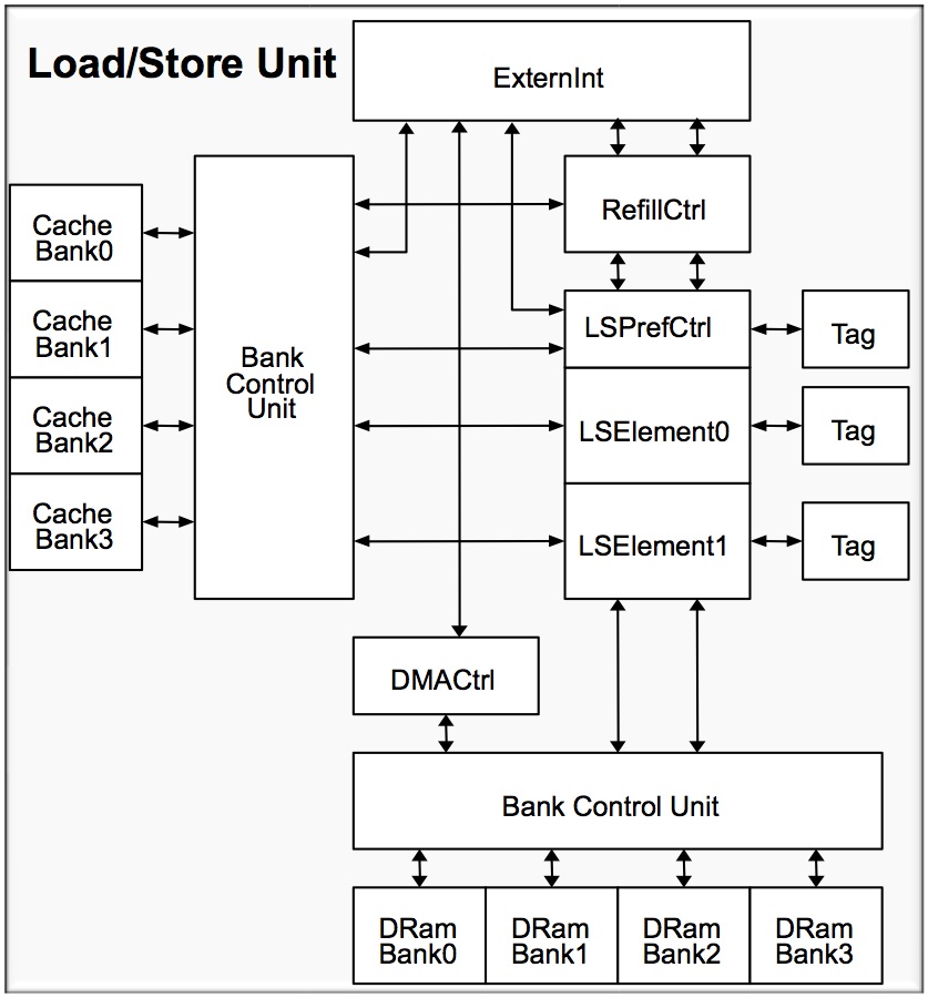
Figure 4. Improved bandwidth through enhanced parallelism is the fundamental focus of the latest generation Xtensa cores' DataRAM Banking control units.
Cadence's bus-enhancement focus extends beyond its own PIF bus. ARM AMBA (Advanced Microcontroller Bus Architecture) AXI (Advanced Extensible Interface) protocol support has been extended to comprehend the v4 standard. And more generally, to improve ease-of-use and acknowledge the notable percentage of Xtensa cores that act as coprocessors to an ARM CPU, Cadence has closely coordinated with ARM to develop debug facilities compliant with ARM's CoreSight access port. To wit, Xtensa 10's and LX5's debug module includes APB (Advanced Peripheral Bus) capabilities, which enable the host processor to manage Xtensa debugging directly through the CoreSight DAP (debug access port).
The company has also made other notable architecture improvements. Chief among them, at least for digital signal processing developers, is the incorporation of an optional IEEE 754-compliant double-precision scalar floating-point unit (FPU) on the Xtensa LX5, along with double-precision floating-point acceleration (albeit not a full double-precision FPU implementation) on the Xtensa 10 (Figure 5). And an expanded suite of FLIX (flexible-length instruction encodings) options now includes 32-, 64-, 96-, and 128-bit instruction alternatives, translating into increased flexibility and potentially higher code density.
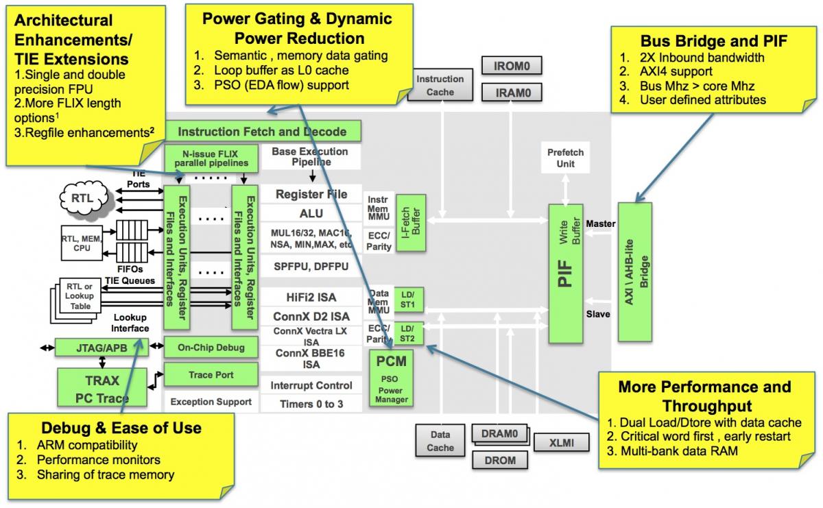
Figure 5. The Xtensa core line has access to an optional double-precision scalar floating point unit in this generation.
According to Cadence, Xtensa 10 and Xtensa LX5 are the first architecture "major releases" since 2010. And revisiting the "application dreams" mentioned at the beginning of this write-up, Rowen asserts that the processors' evolutionary enhancements effectively address these needs by delivering:
- Reduced core and system power consumption
- Boosted data throughput
- Lower latency
- A more flexible memory hierarchy for more flexible programming model, and
- Increased visibility and control for rapid system development and optimization
Apparently at last some potential customers agree. The architectures were developed in conjunction with several lead licensees, one of which has had access to the cores since October 2012 and has already completed an SoC, with initial silicon in hand. More generally, although the architectures were publicly launched in mid-October 2013, the cores have been available for broad licensing since June, and both have already achieved multiple design wins, according to Cadence.
Add new comment