
Intel is widely regarded as being not only the world's largest semiconductor supplier, but also a leading-edge manufacturing process developer and implementer. While foundries such as TSMC are still finalizing their 20 nm processes, for example, Intel has been shipping 22 nm-based production ICs ("Ivy Bridge" CPUs) since May of last year; the company had previously showcased its first 22 nm test wafer at the September 2009 Intel Developer Forum. Intel similarly achieved a several-year production lead on the prior process node (32 nm for itself, 28 nm for foundries). Historically, Intel's processes and fabrication facilities were exclusively used to manufacture its own products. In recent years, however, the company has made its first few forays into the foundry business, in partnership with programmable logic startups.
In October 2010, for example, Achronix Semiconductor reported that it would be leveraging Intel's 22 nm "tri-gate" process to fabricate its FPGAs; Tabula followed up with a similar announcement in February 2012. FPGAs are ideal foundry-relationship catalysts for Intel, first and foremost because the company hasn't made its own programmable logic devices in two decades, so FPGA suppliers aren't Intel competitors. Also, FPGAs are heavily dominated by SRAM structures used to implement LUTs (lookup tables) and embedded memory arrays, making them similar to the SRAMs long leveraged by Intel during process development.
In late February 2013, Intel significantly upped its foundry game, agreeing to make 14 nm-based FPGAs for Altera. And in late June, Altera provided initial details on the first fruits of the Intel partnership, in the form of the upcoming Stratix 10 programmable logic family. Altera was careful to call this a "technology announcement," not a "product announcement," so specifics are still somewhat scant. What the company has shared so far, however, will be of interest for FPGA users targeting digital signal processing and other high-performance applications.
Historically, according to company officials, each process node migration at Altera's longstanding foundry partner, TSMC, has resulted in a roughly 20 percent boost in the raw clock speed of the FPGA fabric. With the two-node jump from TSMC's 28 nm to Intel's 14 nm process, on the other hand, Altera anticipates an estimated doubling of peak clock speed. Altera is also quick to point out that the exclusive (for tier-1 FPGA suppliers) Intel partnership gets Altera's FPGAs to 14 nm much more quickly than would be possible with any other foundry (Figure 1).
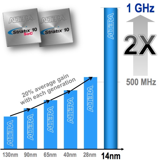
Figure 1. A two-generation process jump, enabled by a foundry partner transition, is projected to deliver a notable performance boost to Altera's FPGAs.
The migration to 14 nm isn't solely about speed, however. Depending on the specific characteristics of a particular FPGA device variant—and of the design implemented in that device—Altera projects that the improvement (compared to today's 28 nm Stratix V) will range from a 2X performance gain coupled with roughly 30 percent higher power consumption, to equivalent performance with a substantial decrease in power consumption—or any point in between (Figure 2).
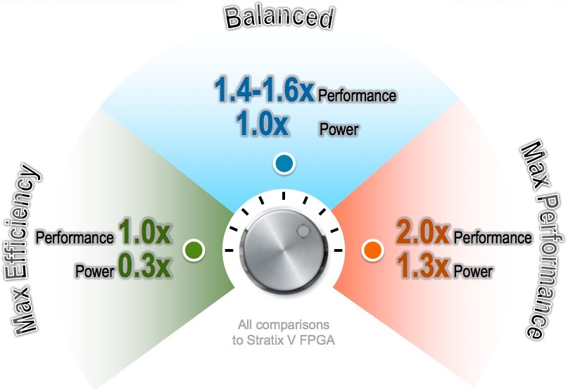
Figure 2. Intel's 14 nm process is both speedy and energy-stingy, thereby providing a range of performance-versus-power consumption options for FPGAs and the designs implemented within them.
Thanks to the available formidable transistor budget of Intel's 14 nm process, Altera forecasts that Stratix 10 FPGAs will more than quadruple the logic capacity of current offerings, extending to greater than 4 million LEs (logic elements) per die. The architecture will be "3D-cognizant," capable of integrating not only multiple dies of FPGA fabric, but also SRAM, DRAM and ASIC function blocks within a single package. Stratix 10 transceivers will double in speed, from 28 Gbps to 56 Gbps. And of particular note to digital signal processing algorithm implementers, Altera forecasts that Stratix 10 will deliver more than 10x the single-precision floating-point throughput of Stratix V, ranging up to greater than 10 TFLOPs (and 100 GFLOPs/watt).
In part, this speed boost is inherently due to the two-node process migration, which increases both the DSP blocks' clock rates and the number of them that can be cost-effectively integrated on a single sliver of silicon. However, Altera has also more fully "hardened" the DSP block architecture; in today's Stratix V, slower generic FPGA logic is leveraged to implement a portion of floating-point functions. Keep in mind that the above performance claims are theoretical maximum estimates; BDTI's recent Stratix V floating-point evaluation (PDF) achieved 162 x 109 (i.e., 1.6 x 10¹¹) FLOPS performance, versus Altera's 1 x 10¹² FLOP estimate for Stratix V. Architecture improvements that boost theoretical maximum single-precision floating-point calculation rates, however, should also increase real-life speeds to a tangible degree.
While the 14 nm partnership with Intel promises to deliver Altera abundant product benefits, for now it will be restricted to the high-end Stratix 10 product line. Altera's mid-range Arria FPGAs will instead migrate to TSMC's 20 nm process for their "10" generation, a move that Altera says will deliver concrete performance and power consumption improvements versus the current high-end Stratix V product line (Figure 3).
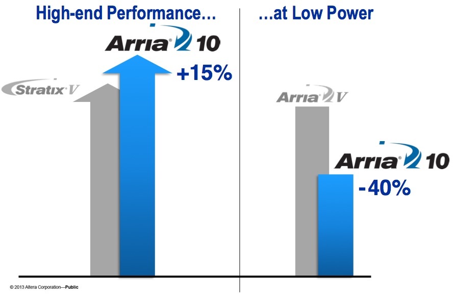
Figure 3. Altera's next-generation Arria 10 FPGAs are predicted to out-perform today's high-end Stratix V offerings, with lower power consumption to boot.
The speed boost extends beyond the FPGA fabric to the dual ARM Cortex-A9 "hard" cores embedded in the "SoC" version of Arria 10. On Arria V and Cyclone V SoC variants, the ARM cores run at 800 MHz. On Arria 10 SoC, they'll receive a 90 percent speed increase, to 1.5 GHz (Figure 4).
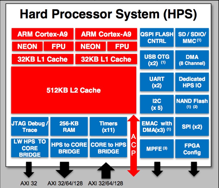
Figure 4. The migration from 28nm to 20nm portends a 90 percent increase in the peak clock speeds of Arria 10 SoC's dual embedded ARM Cortex-A9 cores.
And Altera also has future SoC aspirations for Stratix 10, although company officials currently decline to provide CPU core supplier and product specifics (Figure 5).
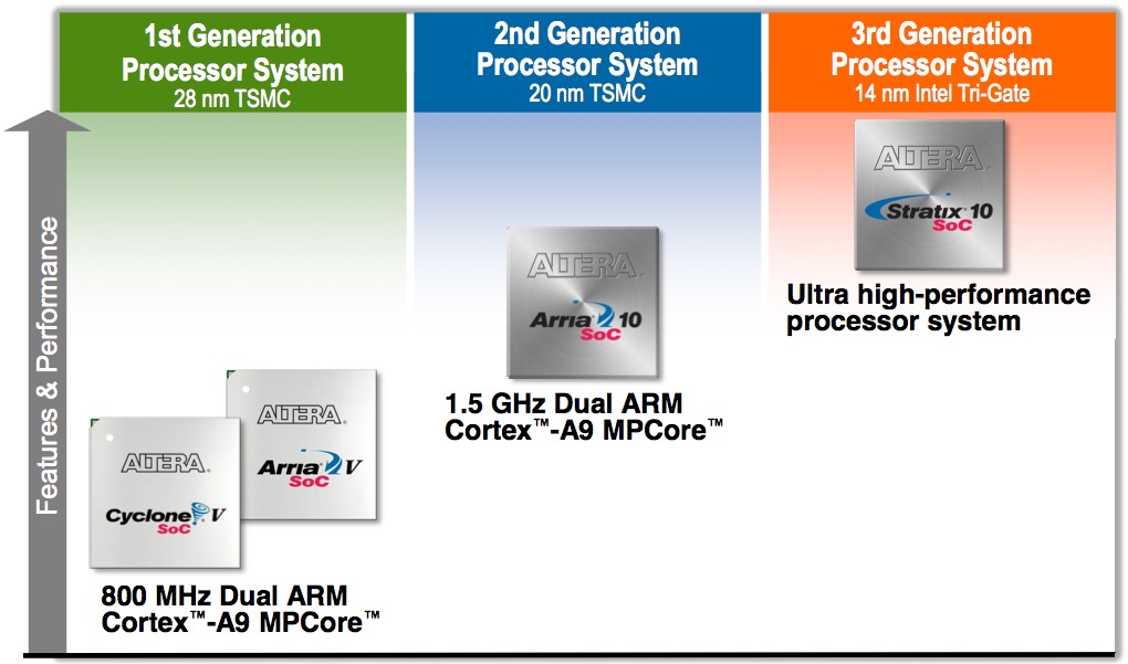
Figure 5. Altera has SoC intentions for the high-end Stratix product line as well, although CPU core details are not yet public.
Speaking of "future," what is the schedule for next-generation products? Altera intends to have initial Stratix 10 test chips in hand by the end of this year, coinciding with Intel's planned production of 14 nm devices. Early-access development software support for Stratix 10 lead customers will follow sometime next year, ahead of sample availability. With Arria 10, early-access design software support is already available; initial product samples are currently forecasted to appear in early 2014.
Add new comment