
Last month Freescale introduced a new baseband accelerator chip for wireless infrastructure equipment. The chip is tailored to the high data rates and computational demands of emerging wireless standards, including 3G-LTE, TDD-LTE, HSPA+, and WiMAX. The accelerator, called the MSBA8100, is designed to run alongside Freescale’s MSC8144, which is a high-performance quad-core DSP processor chip. Together, the two chips are intended to provide a full baseband solution and potentially eliminate the need for FPGA- or ASIC-based acceleration.
The 90 nm MSBA8100 includes specialized hardware to accelerate turbo and Viterbi decoding (up to 120 and 85 Mbps, respectively) and various flavors of
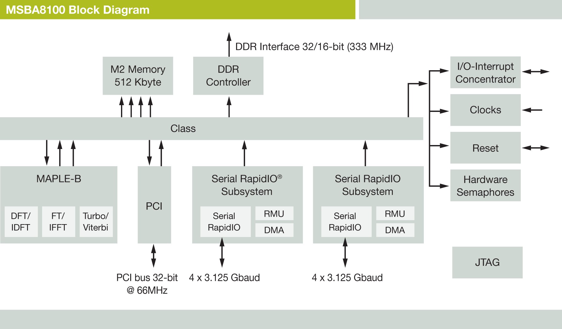
Figure 1. Block diagram of MSBA8100 accelerator chip.
(Graphic courtesy of Freescale.)
The MSC8144/MSBA8100 combo is programmed using the
Freescale’s dual-chip basestation solution makes some good compromises. Many engineers would prefer to have all the basestation processing implemented using only programmable DSP processors so they’d only have one type of processor to program and debug—but basestation processing demands are just too challenging for today’s mainstream processors. There are a few massively parallel processors that might be able to do the trick, but these processors tend to be from relatively small companies without proven track records—or proven development tools and methodologies. (PicoChip is a notable exception here, having shipped chips for 3G cellular and WiMAX base stations for some time.) That leaves FPGAs and ASICs as the most widely used alternatives. FPGAs are much harder to work with than programmable processors, leading to higher development costs and longer schedules. ASICs suffer from inflexibility, and have become increasingly expensive to design.
In this context, coupling a programmable processor (the MSC8144) to an accelerator with a programmable data interface is a reasonable strategy. An open question, however, is whether the co-processor is flexible enough to adapt to changing standards, and whether the associated development tools will make this adaptation straightforward.
Freescale’s dual-chip approach plays the middle ground between a fully homogeneous solution and a multi-technology solution (e.g., processor plus FPGA). This approach may prove attractive to system designers, though much will depend on the chip’s cost and energy efficiency—neither of which have been disclosed yet by Freescale. Freescale has also released very little specific performance information, except to say that the MSBA8100 accelerator supports up to 20 MHz 3G-LTE eNB.
For now, the MSC8144/MSBA8100 combination appears to be an interesting approach, but more concrete information is needed in order to make meaningful comparisons with the alternatives.
Add new comment