
Stream Processors, Inc. (SPI) this week unveiled its data-parallel processor architecture and announced two chips based on the architecture. According to SPI, its architecture is optimized for compute-intensive embedded applications which exhibit a high degree of data parallelism, such as video and imaging. SPI believes that cost-performance and developer productivity advantages will enable its chips to compete successfully against FPGAs, high-end DSPs, and ASICs in these applications.
SPI’s “stream processing” architecture is derived from an architecture developed by the “Imagine” research project at Stanford University. It consists mainly of a host CPU and a SIMD-oriented coprocessor (dubbed "Data Parallel Unit" in Figure 1.) The host processor runs the bulk of the application code, and offloads compute-intensive tasks to the coprocessor. The coprocessor is organized as clusters of ALUs. Each cluster, called a “lane,” contains five ALUs. Operations for the ALUs within a lane are specified in a VLIW fashion. Across lanes, operations are controlled in a SIMD fashion, so that in a given instant, each lane performs the same set of operations as every other lane. Each lane takes its input data from a 16 KB local “lane register file” (LRF); for storage of temporary ALU results, each lane also contains roughly 300 operand registers. The final output is written back to the lane register files, and can be read by the next task executing on the coprocessor. This data-flow-based memory management approach is a natural fit for many DSP applications, which typically involve sequences of data transformations; for such applications, cache-based memory architectures can result in significant amounts of unnecessary data movement.
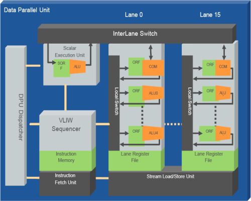
Figure 1. Data Parallel Unit in the SPI architecture, consisting of clusters of ALUs, called "lanes".
To develop an application, the programmer begins with a reference C-language implementation. The programmer then identifies compute-intensive tasks, specifying these tasks and associated data sets using SPI’s extensions to ANSI C. The compiler allocates space for the data sets in the LRFs and schedules the tasks on the coprocessor, managing data synchronization. According to SPI, manual code partitioning across the ALU lanes is not required. If true, this should make programming SPI’s architecture significantly simpler than programming typical multi-core processors. But because SPI’s approach relies extensively on data parallelism, a key challenge for SPI will be to ensure that a sufficiently large subset of a given application is accelerated using the SIMD approach.
SPI is currently sampling SP16-G160 (priced at $99) and SP8-G80 (priced $59) chips running at 500 MHz, and containing 16 and 8 lanes respectively. (All prices in this article are unit prices for 10,000 unit purchases.) SPI also offers software development tools and off-the-shelf software components including video encoders and decoders, such as H.264 and MPEG-4, in addition to low-level DSP and image processing functions.
The SPI devices will likely compete with FPGAs and high-end DSPs. According to SPI, the SP16-G160 can perform H.264 Baseline Profile encoding at 1080p resolution; FPGAs used in conjunction with a host processor have demonstrated similar capabilities. Unfortunately, vendors typically use different algorithm variants, test streams, and metrics when reporting video codec performance, making performance comparisons between the SPI solution and competitors' solutions difficult. However, application development using SPI’s software-based approach is likely to be simpler than development with the hardware-based approach typically used with FPGAs.
The SPI devices will also compete against high-end DSPs and media processors. According to SPI, the SP16-G160 can decode at least two channels of H.264 Main/Baseline Profile at 1080p resolution. In contrast, TI’s DaVinci DM6446 (priced at $35) can decode H.264 Main/Baseline Profile at D1 resolution. Multiple DM6446 chips will likely be required to achieve comparable performance to a single SP16 or SP8 on video applications. For highly data-parallel video applications, SPI’s data-flow based memory organization (requiring fewer non-local data accesses) may also enable the SPI devices to be more energy-efficient than conventional processors.
Processor designers are becoming increasingly aggressive in using parallelism to enable efficient, high-throughput digital signal processing. Many start-ups are employing multi-core approaches, which typically emphasize a mix of task-level parallelism and data parallelism. In contrast, SPI emphasizes data-level parallelism. This is likely to enable SPI to provide a simpler programming model, but may limit the range of applications in which the SPI chips can deliver their full performance potential.
Add new comment