In May 2014, Synopsys expanded its ARC EM licensable processor core product line, which BDTI described as historically being "vanilla" Harvard architecture CPUs with no DSP-optimized features, via the addition of the digital signal processing pipeline-equipped EM5D and EM7D (“D” denoting DSP). This year's follow-on EM9D and EM11D make what at first glance seem to be minor upgrades, in the form of an optional incremental 2-64 KB of special-purpose embedded memory. But, according to company spokespersons Fergus Casey (Senior Manager, R&D) and Angela Raucher (Product Line Manager), the added "XY" memory can lead to up to 3x higher DSP performance in some applications.
Here's what the ARC EM processor family currently looks like (Table 1):
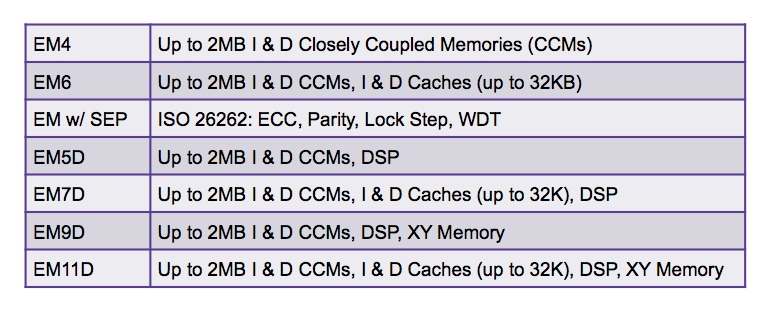
Table 1. Synopsys' ARC EM family members are differentiated by their respective types and amounts of integrated memory, along with the presence (in four cases) of a dedicated DSP pipeline.
As BDTI's July 2014 coverage documents, the key difference between the EM5D and EM7D consists of the latter's inclusion of up to 32 KBytes of data and instruction cache. That same differentiation exists in comparing the EM9D (cache-less) and EM11D (cache-inclusive). They share support for the aforementioned "XY" memory, absent from prior ARC EM family members. "XY" memory is multi-bank, multi-port RAM, optionally implemented as either dedicated memory or a portion of the existing data CCM (closely coupled memory) array, and intended to address DSP applications’ need for fast memory accesses while performing repeated mathematical operations on arrays of numbers (Figure 1). The "XY" memory structure also integrates address generation units (AGUs) and it supports both interleaving and splitting one logical partition into two physical memories supporting even and odd logical words. The address generation units provide addressing modes such as modulo, bit reverse and variable linear offsets.
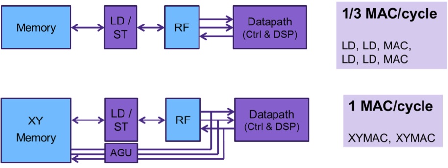
Figure 1. Multi-bank, multi-port "XY" memory can both decrease the number of clock cycles needed to implement an arithmetic operation and improve code density.
As both the above figure and the following table indicate, one key purpose of the "XY" memory array is to reduce the number of cycles required to implement arithmetic operations, both by minimizing the number of required memory accesses and by improving code density (Table 2):
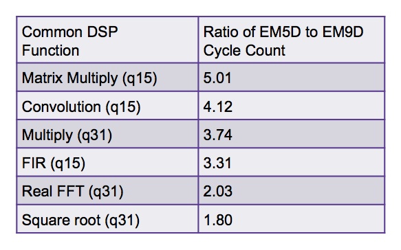
Table 2. Comparative clock cycle counts for various arithmetic functions, showing improvements enabled by multi-bank memory.
And, assuming that the inclusion of "XY" memory doesn't dramatically boost the processor core's power consumption, these improvements also can reduce the per-operation energy consumed by the core at a given clock speed, as a more detailed example provided by Synopsys documents (Figure 2).
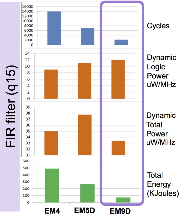
Figure 2. This Synopsys-supplied FIR filter example indicates the performance and power/energy consumption improvements that the company believes "XY" memory provides.
Like other ARC EM family members, the foundation of the EM9D and EM11D is a three-stage pipelined fixed-point CPU. As with the EM5D and EM7D, it's supplemented by a separate, parallel processing pipeline that builds on the ARCv2 ISA with support for more than 100 fixed-point DSP instructions (newly added instructions on the EM9D and EM11D will also be back-ported to the other two EM DSP family members). Hardware elements encompassed in the DSP pipeline include a unified single-cycle 32x32 multiplier/multiply-accumulator, square root, divide and FFT butterfly acceleration units, and a 64+8-bit accumulator configurable as two 32+8 bit accumulators. And optional core extensions available for all ARC EM family members include a single- and double-precision floating-point "assist" engine, a memory protection unit to isolate trusted versus untrusted software, real-time trace and DMA units (the latter allowing allows system resources and peripherals to access memory resources independent of the processor), and a cryptography acceleration engine (Figure 3).
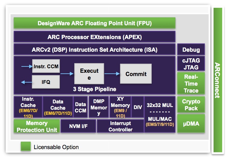
Figure 3. The fixed-point ARC EM architecture can optionally be supplemented by a single- and double-precision floating-point unit, along with other dedicated-function "engines".
Synopsys' Raucher and Casey declined to provide licensing costs for the EM9D and EM11D . However, they did offer the insight that whereas a "typical" EM5D or EM7D core implementation on a 40 nm low-power process takes up approximately 0.03 square mm of die area, a multi-bank memory-inclusive EM9D counterpart fabricated on that same lithography node would consume approximately 0.04 square mm of silicon. The primary motivation for the development of the EM9D and EM11D, they proffered, was the increasing need to simultaneously process inputs from multiple sensors within the CPU core, versus in a separate "sensor fusion" co-processor. With that said, they clarified that the enhanced digital signal processing capabilities of the EM9D and EM11D are primarily focused on audio applications, along with elementary vision processing such as face detection. More involved computer vision tasks (i.e. face recognition) are the bailiwick of a more advanced processor core such as Synopsys' DesignWare EV.
Both Synopsys' and multiple partners' development tools already support the EM9D and EM11D, according to Raucher and Casey. Compilers, for example, will automatically handle any code transformations needed for "XY" memory optimization (legacy compiled code will still run unchanged, albeit not optimally), and are also cognizant of newly added unaligned store capabilities. While historically much industry attention has been focused on DSP core enhancements such as clock speed, pipeline depth, VLIW, and multi-threading support, Synopsys' new ARC EM DSP cores showcase the equally critical necessity to focus on memory accesses in order to optimize performance and power consumption. It'll be interesting to see to what degree the company's benchmark estimates bear out in real-life application implementations, as well as how well "XY" memory enables Synopsys to stand out versus competitors.


Add new comment