
The "Internet of Things" (IoT), one of the hottest topics in technology today, is widely anticipated to be a notable driver of both semiconductor and software demand in coming years. Key to an understanding of the IoT opportunity, as a recent article published on the Embedded Vision Alliance website notes, is its machine-to-machine aspect.
Content generated at the source end of the IoT communication link is created by devices using various sensor technologies, which are forecast to experience rapid increases in adoption rates in the coming years, not only in IoT but also other high-growth markets such as wearable devices (Figure 1).
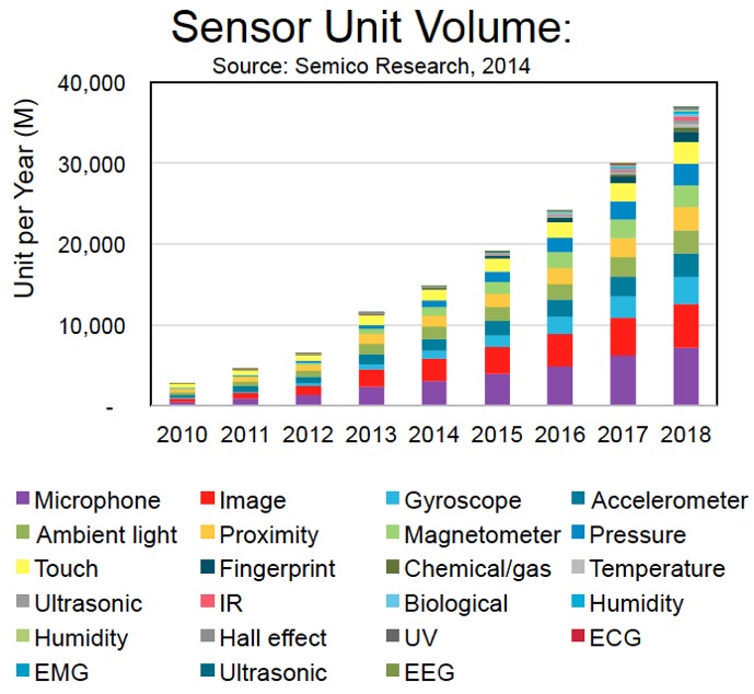
Figure 1. The demand for various sensor technologies in IoT, wearable and other application categories is expected to continue to robustly grow in the coming years.
These sensor technologies can include image sensors, although as Cadence Fellow (and Tensilica founder) Chris Rowen notes, their data "payload" and processing requirements are relatively significant in most cases, therefore more appropriate for pairing with a tailored vision processor such as the company's IVP. Other sensor technologies are more modest in their storage, transfer and digital signal processing needs, and Cadence's recently introduced Tensilica Fusion DSP core was developed with them in mind (Figure 2).
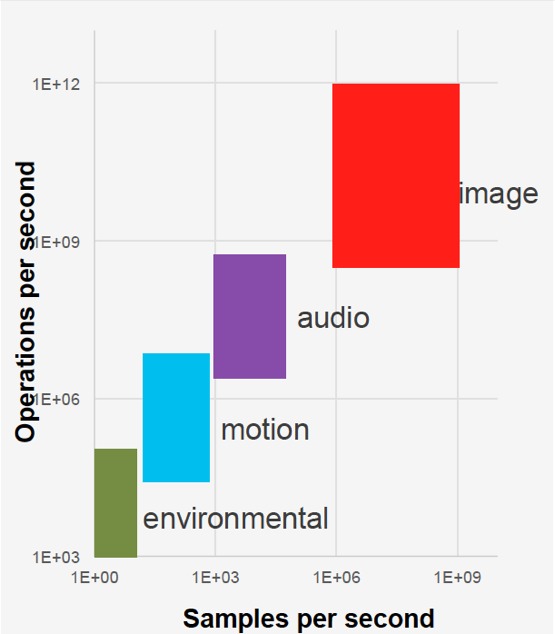
Figure 2. Cadence's new Tensilica Fusion DSP core's single- and multi-sensor focuses extend to entry-level imaging applications.
A key set of functions is common to many applications in IoT, wearable and other similar markets; it includes not only data accumulation and processing, but also the earlier mentioned transfer of results elsewhere, via a variety of communication protocols (Figure 3). These applications' signal processing requirements will inevitably grow in complexity over time, Rowen notes, and energy efficiency is also extremely important.
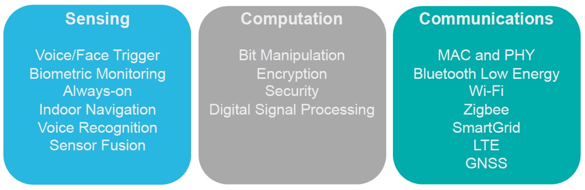
Figure 3. Data acquisition, calculation and communication facilities must all be comprehended when selected a digital signal processor, says Cadence.
The base Fusion architecture combines a two-way VLIW Xtensa processing core supporting three FLIX (flexible length instruction encoding) options, and a MAC alternatively capable of implementing single 32x32, dual 32x16, dual 24x24 and dual 16x16 arithmetic operations (Figure 4). Cadence's customers can optionally build on this Fusion foundation with any or all of five different architecture-extension packages.
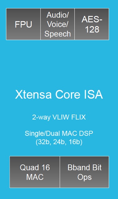
Figure 4. Fusion supplements a two-way VLIW processor-plus-flexible MAC foundation with five optional architecture extension blocks.
The first option package adds two more multipliers, along with additional instructions, to support quad 16x16 MAC capabilities. For even more arithmetic potential, you can also consider integrating the single-precision FPU, whose capabilities operate in parallel with those of the base Xtensa processor core. Additional instruction set support, in the form of the AVS (Audio/Voice/Speech) architecture extension option, enables full software-compatibility with the company's HiFi 3 audio DSP, thereby giving Fusion access to more than 140 HiFi audio/voice software packages.
An AES-128 encryption module is desirable for accelerating narrowband wireless communications standards such as Bluetooth Low Energy and Wi-Fi. The advanced bit manipulation module, meanwhile, accelerates baseband MAC/PHY processing performance. The resultant architecture flexibility, Rowen feels, enables Cadence's customers to fine-tune their particular Fusion implementations for optimum performance, power consumption, silicon area utilization and other parameters in various SoCs and applications (Table 1).
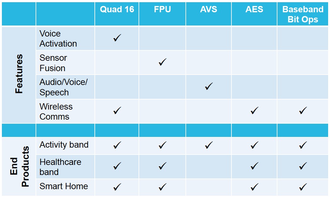
Table 1. Various applications leverage one or more of the Fusion feature set extension options in optimizing for various SoC attributes.
Speaking of parameters, Cadence is being publicly mum at this point about specifications such as clock speeds, operating voltages and current draws, supported process nodes, and transistor counts, aside from a somewhat nebulous performance estimate that the full-outfitted Fusion "approaches 3.5 Dhrystone MIPS/MHz." For more details, you'll need to contact the company directly; the foundation core and its associated package extensions are now available as production RTL.
Fusion's baseline feature set and options appear to be well matched to the target applications. Assuming that its other specifications are also a fit and that the applications themselves are successful, it seems well positioned for robust adoption. With that said, Cadence isn't the only company targeting these application spaces. Competitors include not only other DSP IP providers but also CPU suppliers, whose processor cores are increasingly capable of robust digital signal processing without co-processor assistance. It will be interesting to see how effectively Fusion is able to compete with these alternatives over time.
Add new comment