
In a recent interview in EE Times, BDTI co-founder and president Jeff Bier commented:
Multi-core CPUs are very powerful and programmable, but not very energy-efficient. So if you have a battery-powered device that is going to be doing a lot of vision processing, you may be motivated to run your vision algorithms on a more specialized processor.
Bier could have been speaking about CEVA's MM3101 processing core, which InsideDSP covered in its January 2012 edition. Or he could have been referring to the PVP (pipelined video processing) core inside Analog Device's BF608 and BF608 Blackfin SoCs, discussed in InsideDSP three months later. In both cases, the supplier's intent is that you leverage the imaging-, video- and vision-optimized core's resources to offload the main system processor, translating into higher overall performance and lower aggregate power consumption.
But in this particular case, the occasion of the EE Times interview was the public unveiling of Tensilica's IVP (imaging and video processor), the first such application-focused offering from the company (now in the process of being acquired by Cadence) since the 388VDO Video DSP, introduced five years ago. At the nexus of the IVP is a triple-issue Xtensa core for control processing functions. It's supplemented by (and manages) 32 imaging-tailored "element engines" -- SIMD processors, each capable of up to four simultaneous operations (up to three pixel arithmetic operations, plus up to two pixel data memory references), implemented by the following resources (Figure 1):
- Three 16-bit ALUs
- One 16-bit by 16-bit multiply-add unit
- One 16-bit variable shifter
- Dual 8- or 16-bit load/store units, and
- Multiple register files (data, shift/select, predicate, and alignment)
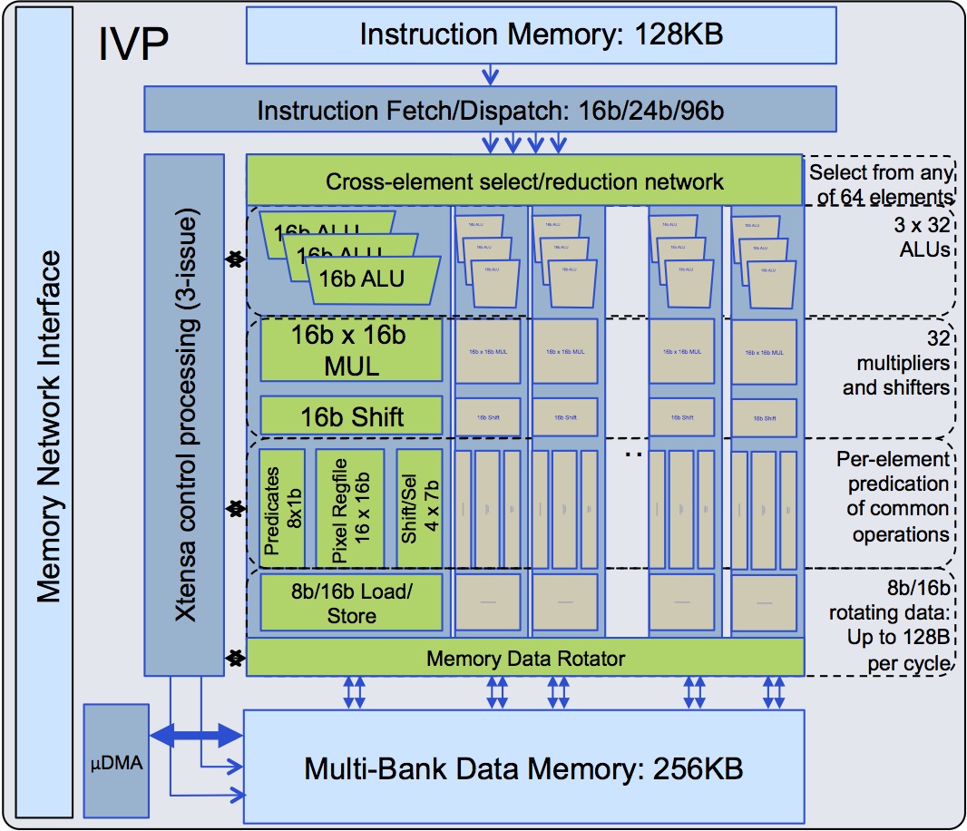
Figure 1. Tensilica's IVP combines an Xtensa processor core with 32 "element engines" each containing commonly used imaging, video, and vision function blocks.
Also included is a 512-bit DMA transfer engine with up to 10 GBytes/second of throughput. In aggregate, the IVP core is capable of up to 96 ALU operations, 32 multiplies, and 64 element loads per clock cycle. And the IVP includes additional resources to help make efficient use of its processing capabilities: data reorganization features include a 64:32 cross-element selection and reduction network, along with a predicated architecture which allows elements to follow different paths through the code. Speaking of code, Tensilica's phase-one ("of a multi-phase plan") software library contains approximately 50 functions and application elements, which Chris Rowen, the company's founder and CTO, describes as "the sum of things that we've found that have been interesting and popular as customers have been porting code and doing benchmarking...we have also followed the general principles of the OpenCV library interface."
Tensilica's Instruction Extension (TIE) methodology was used to develop the IVP's custom-tailored imaging, video, and vision capabilities over a multi-year process that involved benchmarking various core variants against numerous common algorithms. Further instruction set customization by licensees is also possible. Still, all of this silicon potential is for naught if the software development tools are unable to exploit its potential. To this point, Rowen strives to reassure doubters by asserting that the mature SIMD- and VLIW-supportive and native C-based compiler ensures high utilization of both available processing time slots and element engines. Tensilica's toolset also encompasses a debugger and simulator.
From a raw performance standpoint, Tensilica claims that the IVP's potential is "demonstrated by complex algorithm kernels such as motion search and normalized cross-correlation, commonly used in high-precision block and feature matching and optical flow. For a smart motion search on 16-bit data over a 1920x1080 frame with 256x16 pixel search range and 9x3 pixel block size, IVP can achieve a rate of 142 sums of absolute differences per cycle. In addition, a normalized cross-correlation function on 16-bit pixel data with 32-bit accuracy achieves 1 million 8x8 blocks per second." Note that while the IVP can emulate floating-point capabilities, it is fixed point-optimized.
But it's not just about raw performance; many potential applications for the IVP are also power consumption- and price-sensitive. As such, Tensilica's Rowan notes that the company consciously and carefully chose a unique (and his opinion, optimum) combination of speed, die size and flexibility in defining the IVP architecture, in the process evaluating it against alternative processing solutions such as CPUs, DSPs, FPGAs, GPUs and hardwired function blocks. As an example of the results of this optimization work, Tensilica claims (while deftly avoiding any discussion of specific clock speeds), "For an IVP implemented in an automatic synthesis, place-and-route flow in a 28nm HPM [high performance for mobile] process with regular VT [threshold voltage], a 32-bit integral image computation on 16-bit pixel data at 1080p30 [1920x1080 pixel video frames, 30 fps] consumes 10.8 mW. The integral image function is commonly used in applications such as face and object detection and gesture recognition."
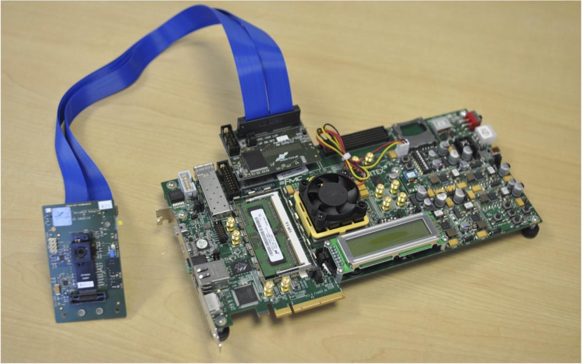
Figure 2. In late February, Tensilica demonstrated the IVP implemented on a 28 nm Xilinx high-end Virtex 7 FPGA.
At late February's Mobile World Congress show in Barcelona, Spain, Tensilica demonstrated the IVP implemented on a Xilinx VC707 (Virtex 7) FPGA evaluation board, mated to an image sensor via a FMC (FPGA mezzanine card) (Figure 2). The company has so far publicly announced four software partners to assist licensees in IVP application implementation: Almalence, Dream Chip Technologies, Irida Labs, and Morpho. Tensilica claims that the IVP is being designed into multiple ASICs now, and that its initial licensees will be in production "within the next few quarters."
Add new comment