
CEVA's DSP cores have long been a fixture in many mobile phone cellular modems, where they handle the tranceiver's digital signal processing functions, working alongside function-specific hardware accelerators. However, the physical layer coordination between the transmit and receiver subsystems, along with overall modem control and other housekeeping tasks, has long been the bailiwick of a real-time CPU core from ARM, Imagination Technologies or another supplier. CEVA aspires to evolve this partitioning with its new CEVA-X baseband processor core family, the first member of which, the CEVA-X4, was unveiled ahead of the February Mobile World Congress (Figure 1).
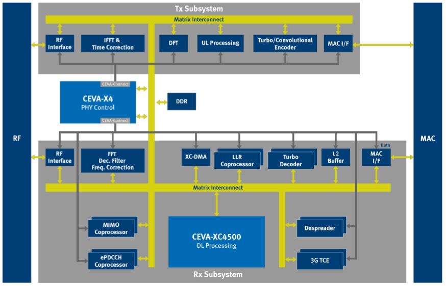
Figure 1. CEVA claims that its new X4 core is capable of handling both physical layer and cellular modem control functions, along with a portion of the transmitter subsystem's digital signal processing needs (in conjunction function-specific hardware accelerators); a separate higher-end CEVA DSP core deals with the receiver subsystem's processing demands.
According to Emmanuel Gresset, Business Development Director for CEVA's Wireless Business Unit, the fundamental factor driving the company's architecture rethink is the combination of higher bandwidth and greater implementation complexity seen with new LTE-A (LTE Advanced) and upcoming LTE-A Pro (LTE-A Release 13 and beyond, also known as "4.5G") cellular networks, in both their data and voice modes. The EVS (enhanced voice services) audio codec used in VoLTE (voice over LTE) deployments, for example, has 4-5x the processing complexity of the legacy AMR (adaptive multi-rate) codec, for example, along with roughly 10x the memory budget. And key to the higher transmission speeds of newer LTE variants is multi-20 MHz carrier bundling and bandwidth aggregation, which according to Gresset introduces significant inter-carrier modem control challenges on top of the need for intra-carrier measurement, calibration and other functions.
Further adding to the implementation complexity is cellular handset manufacturers' insistence that the modem hardware be capable of supporting multiple RATs (radio access technologies), sometimes at the same time (for simultaneous connection to multiple cells), along with support for both leading edge and legacy RATs. Processing performance demands will further increase, of course, with "5G" technologies currently under development. But energy efficiency requirements will be unrelenting. In responding to these requirements, the initial CEVA-X4 family member represents a notable feature set upgrade over its CEVA-X1643 predecessor (Figure 2).
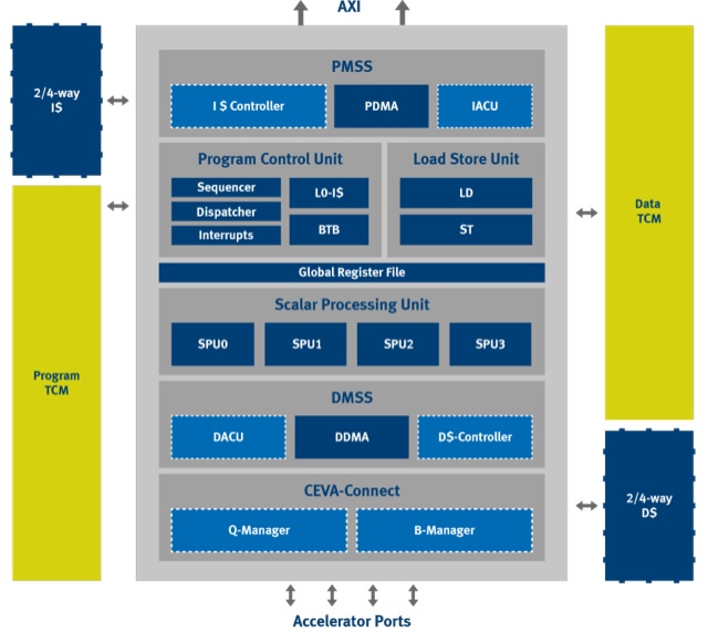
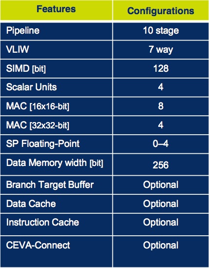
Figure 2. This initial CEVA-X4 member of the new CEVA-X core family (top) contains four SPUs (scalar processing units), along with a mix of other standard and optional features, and local memory variety (bottom).
Focusing first on the digital signal processing capabilities, the CEVA-X4 supports one to four FPUs' worth of optional IEEE-compliant single-precision floating-point arithmetic, a feature absent from the CEVA-X1643 (Figure 3). The CEVA-X4 also doubles the number of 16x16 MACs (to eight) and quadruples the number of 32x32 MACs (to four); as is common, the two MAC types share silicon resources and cannot be concurrently used. Doubled, too, is the SPU (scalar processing unit) memory bus width, to 256 bits; each SPU is comprised of a ten-stage pipeline. And doubled as well is the CEVA-X4’s SIMD parallelism, to 128 bits.
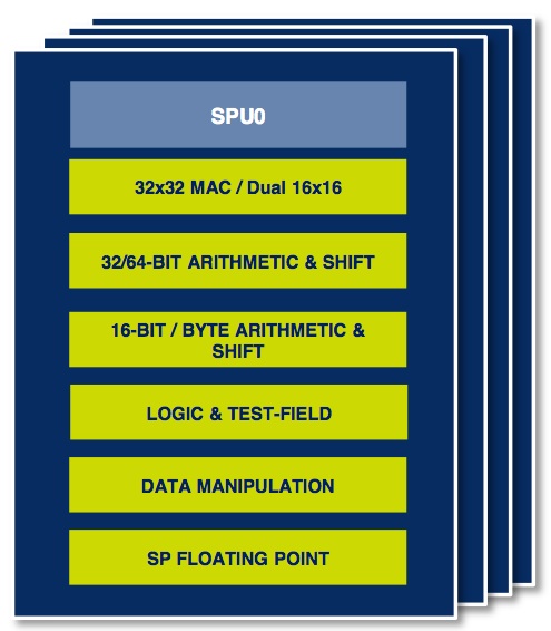
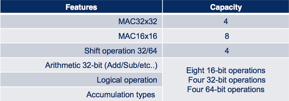
Figure 3. Each SPU (top) integrates a 32x32 MAC also usable as dual 16x16 MACs, an optional single-precision FPU, and additional high-speed arithmetic and other resources (bottom).
In at least one respect, however, the new core is a seeming back-step in DSP capability versus its predecessor, at least on paper. The CEVA-X4 is a seven-way VLIW architecture, whereas the CEVA-X1643 offered eight-way VLIW. However, CEVA's Gresset suggested that the prior architecture's added implementation complexity wasn't justified by software utilization of its potential, providing motivation for the recent simplification and silicon-slimming move.
It's in the PHY layer and overall system control processing enhancements, however, that the company sees its greatest opportunity to grow its silicon footprint, both in an absolute sense and at the expense of competitors. CEVA-X4 offers a greatly expanded control code instruction set, touting zero-latency capabilities for optimal performance on serial code, along with byte support and hardware-accelerated 32-bit multiply and divide operations. Prior static branch prediction facilities have been significantly supplemented by newly added dynamic branch prediction support, including an optional branch target buffer. Fast context switch support improves CEVA-X4's real-time operating system compatibilities, as does its support for supervisor and user modes, semaphores, and other key real-time features.
The CEVA-X4 core can tackle up to eight scalar operations in parallel. Optional L1 program and data caches, each either two- or four-way in form, expand on the direct-mapped program and two-way data (and otherwise more feature-limited) cache support in the CEVA-X1643. The program and data system buses, the latter both master and slave in nature, all have bus widths that areall doubled, to 256 bits wide in each case. Hardware acceleration integration features include multiple optional CEVA-Connect expansion ports, along with hardware queue and buffer managers. And from a raw performance standpoint, Gresset forecasts that CEVA-X4 will run at up to 1.5 GHz in a 16 nm process, with peak dynamic power consumption measuring only 0.05 mW/MHz (potentially even less, depending on fabrication process specifics).
CEVA's Gresset acknowledges that porting code from an existing ARM Cortex-R7 or equivalent control processor to CEVA-X4 isn't a risk-free proposition for a customer, but CEVA believes that the savings in with the licensing fees, silicon area and power consumption from combining multiple cores into one will be attractive. Gresset also believes that the superscalar and out-of-order capabilities supported by conventional CPUs are unnecessary in baseband processing; their elimination in CEVA-X4 is a key factor in the company's claimed significant die and power savings. ARM would likely disagree with CEVA's "unnecessary" assessment; in fact, the company chose Mobile World Congress as the occasion to unveil its latest Cortex-R8 offering targeting (among other things) various cellular modem control tasks.
A separate high-end DSP core such as the company's vector-enabled CEVA-XC4500 will still be necessary to handle receiver subsystem processing tasks, which tend to be significantly more complicated than their transmitter subsystem equivalents. CEVA plans to leverage the new CEVA-X architecture framework as the foundation not only of the initial CEVA-X4 but of future CEVA-X and CEVA-XC products as well. Gresset alluded to one such upcoming core, a lower-end variant due later this year which will contain only a single SPU and, like the recently introduced CEVA-XC5 and CEVA-XC8, will target IoT and other low-data-rate LTE MTC (machine-type communications) applications. Nearer term, the CEVA-X4 is available for licensing, with initial partners' SoCs containing the core anticipated to appear within a year.
Add new comment