
Automobile-based processing intelligence, both in the form of fully autonomous vehicles and more modest ADAS (Advanced Driver Assistance Systems), garnered exclusive billing in NVIDIA's keynote and booth at this year's Consumer Electronics Show, held last month in Las Vegas, Nevada. The information presented highlighted the growing importance of automotive applications not only to NVIDIA and its semiconductor competitors, but also to their shared customers as well as to their customers, i.e. vehicle owners and drivers. And it centered on a new NVIDIA Tegra SoC, as-yet formally unnamed but referred to here by its likely "Parker" project name.
You may know NVIDIA primarily as a developer of graphics processors for mobile and desktop computers, along with supercomputers (where they primarily find use as co-processors for algorithm acceleration), and in fact such products generated 85% of the revenue reported in the company's most recent earnings release. However, NVIDIA also sells a line of ARM-based application processors called Tegra, with a lineage stretching back to the company's early 2007 acquisition of PortalPlayer, and which it has historically sold primarily into smartphones, tablets and other mobile electronics devices.
Unfortunately, the company has garnered limited success in these traditional SoC markets versus competitors such as Intel, MediaTek, and Qualcomm. However, according to Senior Automotive Director Danny Shapiro, who BDTI interviewed subsequent to CES and the Detroit Auto Show, the company has high hopes that steadily maturing automobile autonomy, coupled with drivers' and passengers expanding desires for both entertainment and information during commutes, will deliver the success story that Tegra has long sought.
NVIDIA’s automotive aspirations first became clearly evident at the January 2014 CES keynote, where the company unveiled two planned versions of its Tegra K1 architecture. The first, more conventional in implementation, combined four ARM Cortex-A15 primary cores with a fifth lower power (and lower performance) "battery saver" Cortex-A15. Conversely, the latter Tegra K1 variant, notably used in the HTC-developed and Google-branded Nexus 9 tablet, replaced the five-Cortex-A15 cluster with two custom 64-bit NVIDIA CPUs, known solely by their "Project Denver" code name.
NVIDIA has said little publicly about Project Denver, but it's believed to employ a very wide in-order superscalar pipeline, leveraging both hardware decoder and software-based binary translation (i.e. dynamic recompilation) in order to implement a variety of CPU instruction sets, analogous to Transmeta's past "code morphing" approach to emulating the x86 architecture. In fact, some industry observers believe that Project Denver's original intent was to compete against AMD and Intel x86 CPUs as an extrapolation of NVIDIA's nForce chipset program, although Project Denver now solely focuses on implementing the ARMv8 64-bit instruction set.
Last year's CES brought even more focus on automotive, in the form of the Tegra X1 SoC and two associated system modules, DRIVE CX and DRIVE PX. Tegra X1, fabricated on TSMC's 20 nm process (versus the 28 nm node leveraged by the precursor Tegra K1 family), marked a return to standard ARM core-based application processor design in combining four Cortex-A57 primary cores and four Cortex-A53 secondary cores. Like Tegra K1, it harnessed a CUDA-compatible GPU core, this time a Maxwell-generation offering versus the predecessors' Kepler-generation GPU. The DRIVE CX module, intended for next-generation vehicle infotainment systems, is offered in versions based on either Tegra K1 or X1. And the dual Tegra X1-based DRIVE PX module can be fed by up to twelve camera inputs and implements driver assistance and autonomous driving intelligence.
Demonstration videos of DRIVE CX and DRIVE PX from CES 2015 can be found on the Embedded Vision Alliance website.
- NVIDIA Demonstration of its Drive CX ADAS Platform for Surround Vision
- NVIDIA Demonstration of its Drive PX ADAS Platform for Object Identification
- NVIDIA Demonstration of its Drive PX ADAS Platform for Surround Vision
- NVIDIA Demonstration of its Drive Studio Development Tool
This year's CES delivered no upgrade to DRIVE CX, although Shapiro indicated that this omission was solely due to NVIDIA’s desire to tightly focus its messaging, and that a DRIVE CX 2 update is a matter of "when, not if". Autonomous driving got sole attention this time, in the form of the enhanced DRIVE PX 2 module and its unnamed new application processor foundation (Figure 1). Back in 2013, prior to the release of the Tegra X1, NVIDIA's public roadmap showed an upcoming SoC code-named "Parker" that was based on a Project Denver CPU core, along with a Maxwell GPU core, and was to be fabricated in a FinFET process. BDTI believes that the new SoC used in drive PX 2 is “Parker,” but NVIDIA declined to confirm this.
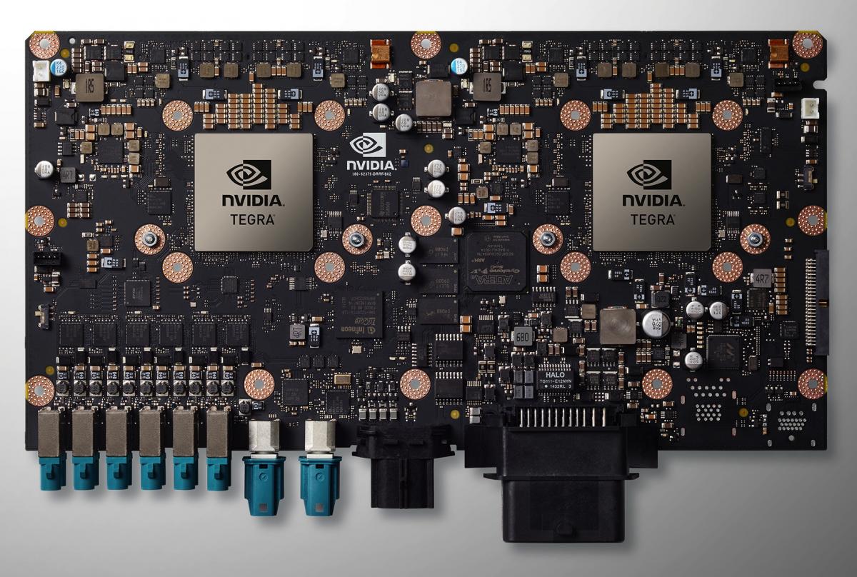
Figure 1. DRIVE PX 2, combining the processing resources of a new SoC (top) and optional external graphics boards (bottom), represents NVIDIA's latest solution for autonomous driving.
The 16 nm-fabricated "Parker" SoC deviates from a conventional "big.LITTLE" multi-core approach by combining two primary-core architectures (four Cortex-A57 cores and two Project Denver cores) within a single SoC. The CES unveiling exclusively focused on one particular variant of the associated DRIVE PX2 module, combining two "Parker" SoCs with two MXM (Mobile PCI Express module)-based external graphics boards, each leveraging a Pascal GPU. However, Shapiro subsequently revealed that "Parker" also integrates an on-chip GPU, of unspecified architecture (likely Maxwell) and capabilities. More generally, Shapiro indicated that the DRIVE PX2 module family ranged from one to four "Parker" SoCs in size, along with optional off-chip graphics boards, dependent on a particular customer's processing requirements.
NVIDIA believes that the dual-"Parker", dual-Pascal DRIVE PX 2 variant will represent a substantial potential-performance upgrade over today's DRIVE PX (Table 1):
|
|
DRIVE PX |
DRIVE PX2 |
|
SoCs |
2 |
2 |
|
External GPUs |
0 |
2 |
|
CPU cores |
8 ARM Cortex-A57, 8 ARM Cortex-53 |
8 ARM Cortex-A57, 4 Project Denver |
|
GPU cores |
2 Maxwell |
2 unknown (internal), 2 Pascal (external) |
|
FP32 TFLOPS |
>1 |
8 |
|
INT8 "Deep Learning Tera-Ops" |
2 |
24 |
|
TDP |
Unspecified |
250W |
Table 1. Specification Comparisons Between NVIDIA DRIVE PX Generations
Note in the above table that NVIDIA has begun specifying a new performance metric, the "Deep Learning Tera-Op", which the company declined to describe at CES but Shapiro subsequently explained as the number of 8-bit simple integer operations delivered by a particular SoC or system architecture. Note, too, the substantial 250 W estimated power consumption of this particular DRIVE PX 2 configuration. Another view of the system board, this time with the liquid cooling structure attached, suggests that the MXM graphics boards will generate the bulk of the heat, and Shapiro suggested in the interview that a "Parker"-only configuration would likely be able to dispense with liquid cooling (Figure 2).
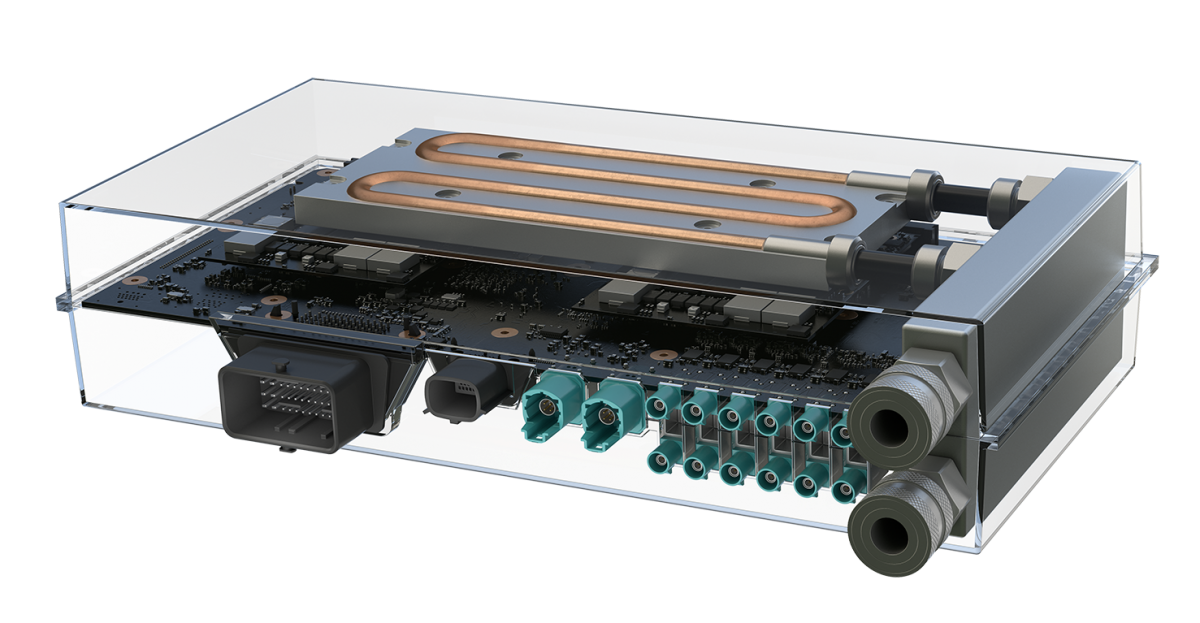
Figure 2. DRIVE PX 2's external cooling configuration suggests that the optional discrete graphics ICs will represent the predominant heat sources.
NVIDIA will have limited availability of DRIVE PX 2 for early customers next quarter, with more widespread availability in the fourth quarter. NVIDIA also announced at CES that Volvo will be using Drive PX 2 (along with software from fellow Embedded Vision Alliance member ADASWorks) as the basis of its autonomous vehicle public pilot program set to begin in 2017. The attention devoted to "Parker" and DRIVE PX 2 at CES clearly suggests that NVIDIA views automotive applications as key to the company's ongoing success. For more information, see the following video captured by the Embedded Vision Alliance at CES 2016:
Add new comment