
"There's been at least one DSP core in every chip that Qualcomm's ever made." Qualcomm senior director of product management Rick Maule used this statement as his lead-in to an explanation of the latest-generation QDSP6 architecture, specifically where it fits in the company lengthy DSP development heritage. QDSP6, if you haven't already figured out, refers to Qualcomm's sixth-generation DSP core architecture and is also commonly referred to by its "Hexagon" marketing moniker. The sixth-generation classification further subdivides into multiple versions; QDSP6 V2, for example, was recently benchmarked by BDTI, with both fixed-point, single-core (PDF) and predicted fixed-point, multi-thread/core (PDF) BDTImark2000 results published on BDTI's website. Meanwhile, as you'll soon see, QDSP6 V5 appears to be well along in development within Qualcomm.
Its immediate precursor, QDSP6 V4, is the most recent variant to enter volume production, integrated within the company's 28 nm Snapdragon 4 SoCs, which InsideDSP covered in detail last fall (see "NVIDIA and Qualcomm ARM Up Against Competitors") (Figure 1).
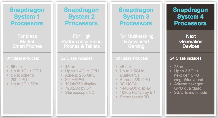
Figure 1. The Qualcomm Snapdragon SoC product line, now in its fourth generation, has experienced three lithography shrinks as well as single-to-multi core CPU migrations, GPU and DSP enhancements, and other improvements
QDSP6 V4 has another important distinction; it marks the first time that Qualcomm has opened up DSP core programming to customers and developer partners via a software development kit that's currently in beta testing. Qualcomm has also focused on bolstering the core's compatibility with, and cognizance by, common compilers and other coding resources such as GCC and LLVM. Specifically, the company is enabling programming of the DSP core in the Snapdragon SoCs' multimedia processing subsystem; the twin DSP cores in the modem subsystem remain exclusively for use by Qualcomm itself (Figure 2).
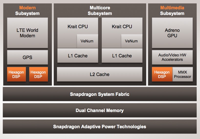
Qualcomm's 28 nm Snapdragon 4 SoCs contain three QDSP6 V4 DSP cores, one of which (in the multimedia subsystem) is now programmable by Qualcomm customers and developers
To date, Qualcomm has not provided extensive public disclosure on QDSP6 architectural details, but the data that the company has shared is intriguing. The Hexagon feature set extends beyond that of a "pure" DSP, including support for symmetric multiprocessing, a memory management unit and a hypervisor. These control-flow and other CPU-like attributes enable it to more fully offload processing tasks from the Snapdragon CPU and/or GPU cores (a standalone operation capability which Maule referred to as "fire and forget"). And it's also multi-threaded, as published power consumption results for QDSP6 V3 reveal (Figure 3).
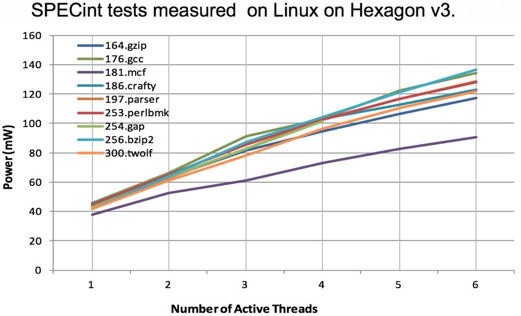
Figure 3. QDSP6's VLIW multi-threaded architecture leads to a near-linear thread count-versus-power consumption pattern, excluding the power draw of foundation circuitry such as bus interface logic
Qualcomm's Maule stressed that QDSP6 is a true VLIW architecture with predictable per-thread behavior. The above graphic indicates that some amount of thread-independent foundation circuitry exists that consumes power above and beyond that of the thread-specific logic. However, in a real-life situation in which no threads were currently being processed, the Snapdragon SoC's elaborate power management scheme would eventually clock- and power-gate the QDSP6 core, effectively shutting it off until it was again needed in the future.
QDSP6, like the Snapdragon SoCs that house it, began its life on the 65 nm process node. Subsequent versions on 45 nm and (now) 28 nm lithographies delivered increased transistor budgets that Qualcomm harnessed to make various architecture enhancements, including increasing the amounts of integrated L1 and L2 cache and bolstering the core's multi-threading facilities. The first instantiation of QDSP6 V4 runs at 500 MHz, versus 400 MHz for the QDSP6 V3, and contains 16 KByte L1 and 256 KByte L2 caches (Figure 4).
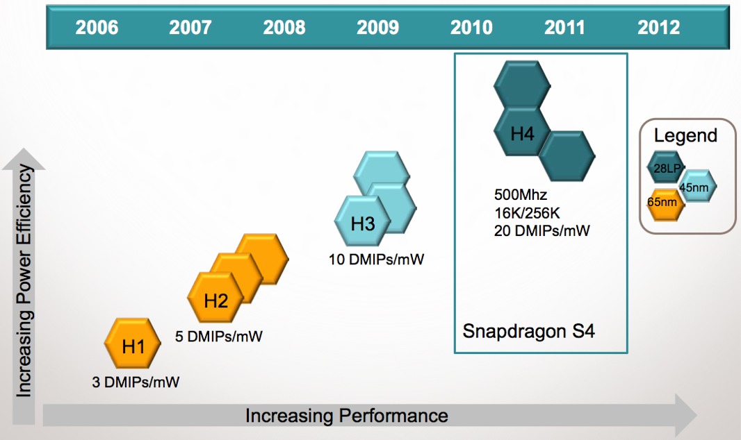
Figure 4. Qualcomm's QDSP6 roadmap reveals performance improvements driven by both lithography shrinks and architecture tweaks, balanced against a comparable focus on reducing power consumption. H1, H2, H3 and H4 reference Hexagon i.e. QDSP6 V1, V2, V3 and V4. The multiple H2, H3 and H4 symbols in the graphic reflect multiple iterations of these particular QDSP6 versions, with varying amounts of on-core cache, etc.
Qualcomm's Maule stressed that, given that the Snapdragon SoCs' predominant use in battery-operated systems (versus, say, a DSP core for a powerline-fed base station SoC), a focus solely only on performance improvements from generation to generation, and from version to version within a generation, wouldn't have been appropriate. As the above figure indicates, power efficiency and performance improvements have been equally important, and the company believes it's made notable strides in both areas. Qualcomm claims 20 Dhrystone MIPS/mW on QDSP6 V4 versus 10 DMIPS/mW on the QDSP6 V3 predecessor, 5 DMIPS/mW on QDSP6 V2 and 3 DMIPS/mW on the initial QDSP6 version.
At the January IEEE International Conference on Emerging Signal Processing Applications (IEEE-ESPA), Dr. Raj Talluri, Qualcomm's Vice President of Product Management, used portions of his plenary talk to showcase key target applications for the QDSP6 architecture. Some of them were predictable case studies of already-established DSP opportunities: audio processing (encoding, decoding, transcoding, noise cancellation, bass boost, virtual surround and other enhancement functions), along with various types of still image and video processing tasks. The increasingly ubiquitous H.264 video codec received particular showcase, for example: according to Qualcomm, the combination of new instructions and cache enhancements has increased the architecture efficiency (measured in millions of cycles per second) necessary to decode a representative compressed bitstream (Figure 5).
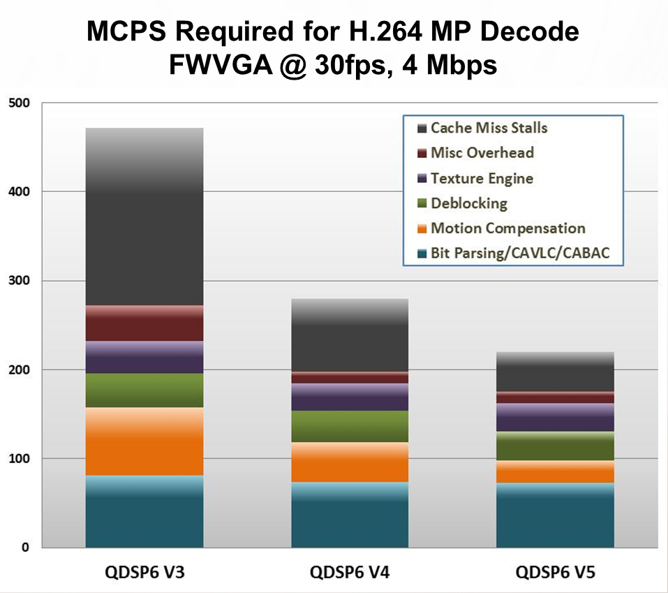
Figure 5. Version-to-version instruction set, cache and other enhancements make QDSP6 V4 an increasingly efficient "engine", as measured in millions of cycles per second, for decoding H.264 video bitstreams, according to Qualcomm (CAVLC = content-adaptive variable-length coding, CABAC = context-adaptive binary arithmetic coding)
You might reasonably infer from the above figure that QDSP6 V5 is on the way. Maule declined, however, to indicate when it might be available in SoC form, on what process node it might first appear, what clock speed it would run at, etc.
Other highlighted applications in the IEEE-ESPA presentation were more trendsetting. Talluri mentioned, for example, the conversion between 2-D and 3-D versions of a polygon- or pixel-based image or video, for appropriate-format output to an integrated or tethered display. He also noted the execution time and power consumption improvements that could be garnered by migrating an augmented reality application from a 100% CPU-based approach to one that fully leverages the integrated QDSP6 V3 DSP core (Figure 6).
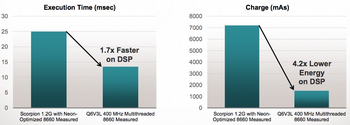
Figure 6. Offloading appropriate portions of an augmented reality algorithm to QDSP6 not only frees up CPU core horsepower but also improves processing speed and decreases overall SoC power consumption, according to Qualcomm
BDTI is currently running benchmark studies on QDSP6 V4 and will analyze the comparative results versus already-published QDSP6 V2 metrics, as well as discuss specifics of the Qualcomm-supplied software development kit, in an upcoming issue of InsideDSP. It will be interesting to see how the V2-versus-V4 results on BDTImark2000 stack up against the comparative performance claims that Qualcomm has already published for these QDSP6 generations.
Add new comment