
Look back over the history of processors, and you'll see many examples of tasks initially restricted to running on high-end processors that, once they became popular and standardized, eventually attracted specialized co-processor or processor support (Figure 1). Consider, for example, video encoding and decoding, nowadays efficiently handled by a multimedia co-processor core sitting alongside the main processor in a SoC. Or consider graphics processing; initially, only BitBlt and other bitmap-level functions were hardware-accelerated, later followed by 2D graphics operations, but now pretty much the entire 3D pipeline is handled by a dedicated graphics processor. Wave Computing forecasts that a similar evolution will occur for deep learning, and in response has introduced its DPU (dataflow processing unit) architecture, focused initially on initial model training.
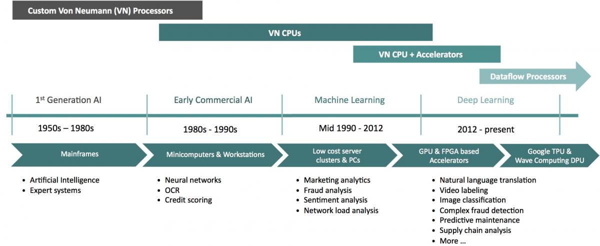
Figure 1. Wave Computing aspires to be the latest beneficiary of the longstanding trend of functions migrating from general-purpose processors to specialized hardware.
The general- to special-purpose processor evolution is already well underway for deep learning, at least for inference (when a neural network analyzes new data it’s presented with, based on its previous training), judging from the latest client-side processor and core announcements from companies such as Cadence, CEVA, Movidius, and Synopsys. Server-side inference is also common, and Google has responded by developing the TPU (Tensor Processing Unit) to accelerate inference using the company's TensorFlow deep learning framework. FPGAs are also increasingly finding use as deep learning inference accelerators.
What, though, about the initial model training process that precedes inference? To date, most hardware acceleration here has been done using GPGPU (i.e. "general-purpose computing on graphics processing units"), leveraging GPUs' massively parallel processing architectures in conjunction with their floating-point arithmetic capabilities. However, according to Jin Kim, Ph.D., Wave Computing's Vice President of Marketing and Business Development, conventional heterogeneous processors such as GPUs aren't ideal for deep learning computations. Deep learning networks, he notes, are constructed from dataflow graphs and programmed using deep learning software. Repetitive bidirectional data transfers and parallel-to-serial-to-parallel bottlenecks between the system CPU and GPU are examples of the overhead incurred when converting between a dataflow graph and sequential threads running on a GPU. The outcome, with the GPU in this case acting as a deep learning training co-processor versus a mostly-unidirectional data flow processor, is performance-inefficient no matter how high performance the link between the CPU and GPU, Kim opines (Figure 2).
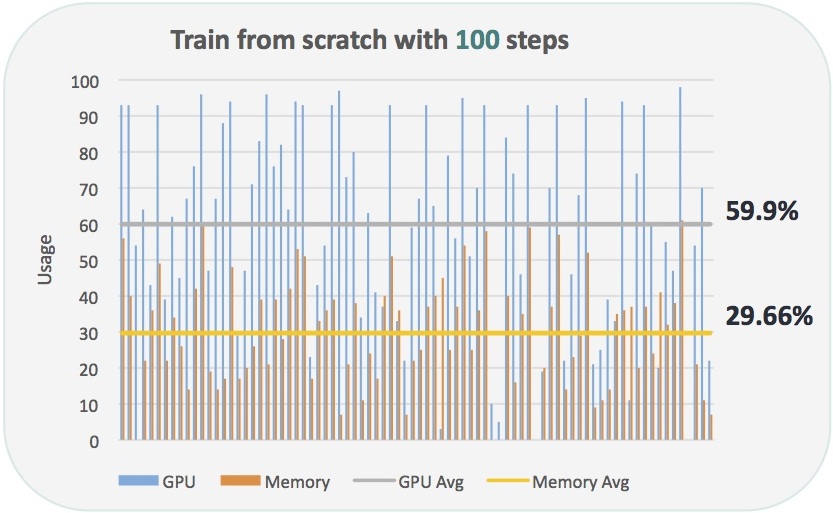
Figure 2. Bidirectional transfer bottlenecks between a CPU and GPU, along with a limited inability to retain instructions and data on-GPU for reuse, hamper its effectiveness as a deep learning training accelerator, according to Wave Computing (results shown are from the company, and for TensorFlow v0.9 training the Inception V3 model on a NVIDIA GTX980 "Maxwell" GPU)
It's preferable, Kim believes, to directly compile the deep learning network dataflow graph to a Wave Computing-optimized graph, which can then be run directly on the DPU, which is optimized for dynamic instruction reconfiguration in conjunction with on-chip data persistence. According to Kim, the company initially targeted any "heavy data crunching" application, aiming for a chip that was less expensive than developing an ASIC while offering a higher-level programming abstraction compared with FPGAs. Two years ago, after Wave Computing successfully completed its initial 28 nm test chip and raised additional funds, it decided to focus specifically on deep learning.
At the heart of the DPU, according to Chris Nichol, the company's Chief Technology Officer, is the PE (processing element), along with accompanying tightly coupled instruction and data RAM (Figure 3). PEs, he explains, are statically scheduled and self-timed dataflow processors capable of functions such as multiplexing (i.e. input selection), as well as input-to-output steering and fan out. They cannot do conditional branches, as a conventional RISC core might, but they can conditionally execute code, read and write memory, handle logical compare and arithmetic add operations, etc. They are a type of CGRA (coarse-grained reconfigurable architecture), in this case with instructions programming the reconfigurable elements. And they can both coordinate with neighboring PEs in a SIMD fashion or operate separately in a MIMD arrangement.
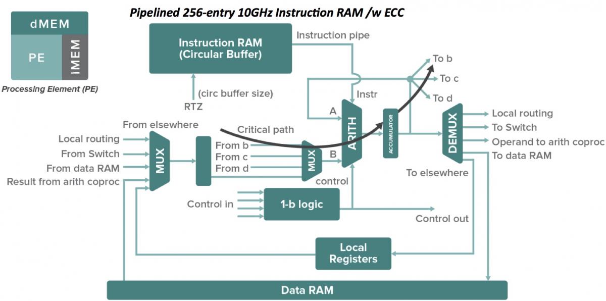
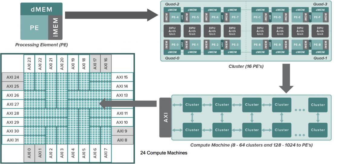
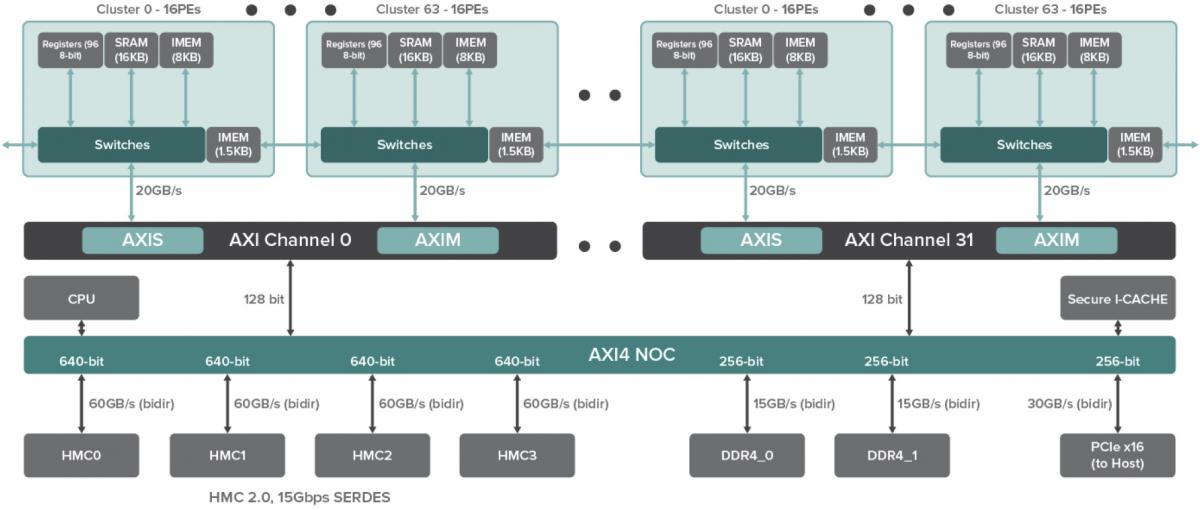
Figure 3. The PE (processing element) and arithmetic unit (top) are at the computational heart of the DPU, combining to form clusters and then compute machines (middle). The chip's memory architecture is similarly distributed and hierarchical (bottom).
Each pair of PEs shares an expanded-function arithmetic unit, containing an (8-bit x 8-bit + 16-bit) multiplier-accumulator, along with wide CLA (carry-lookahead) adders, barrel shifters, and other functions such as leading-zero and ones counters. MACs can be dynamically combined as needed to construct wider multipliers up to 32-bit x 32-bit + 64-bit in size. Note that the DPU fundamentally supports 16-bit fixed-point arithmetic with stochastic rounding; unclear at this point is to what if any degree the lack of inherent floating-point capabilities will hamper its deep learning acceleration aspirations. Newer frameworks such as Google's TensorFlow, Microsoft's Cognitive Toolkit (formerly CNTK), and Facebook's proprietary framework are inherently 16-bit fixed point-friendly, according to Kim. He acknowledges, however, that older (and today, more popular) PC-spawned frameworks such as Caffe remain floating-point-centric, thereby explaining the increasing prevalence of architecture-optimized floating-to-fixed-point model conversion utilities. For now, Wave Computing is focusing its software development and marketing energy on TensorFlow, while remaining framework-flexible from a silicon standpoint.
Sixteen PEs and eight associated arithmetic units combine to form a cluster. The next level of DPU architecture granularity is the Compute Machine, which combines between 8 and 64 clusters (i.e. 128 to 1,024 PEs, programmable at boot time). And at the chip level, there are 24 Compute Machines, interconnected to each other and to the outside world via AXI links (Advanced eXtensible Interface, the third-generation ARM-championed and open-standard AMBA Advanced Microcontroller Bus Architecture). Memory is similarly hierarchical in the DPU architecture, beginning with the PE-coupled instruction and data memories and registers, and expanding outward to an integrated instruction cache and dual 256-bit DDR4 SDRAM controllers, along with four 640-bit HMC (hybrid memory cube) interfaces. Also included is a 32-bit Andes Technology N9 microcontroller for booting and inter-cluster supervision functions; the bulk of coprocessor management tasks are the bailiwick of a separate host CPU interfacing to the DPU over a third-generation PCI Express x16 interface.
The 16 nm-fabricated production chip has just taped out, with first silicon due back from TSMC by the end of this year. The target clock speed is up to 10 GHz (8 GHz nominal), with sub-200W peak power consumption. Raw per-chip resource specifications are notable:
- 16,384 PEs
- 8,192 arithmetic units, each containing an (8-bit x 8-bit + 16-bit) multiplier-accumulator
- 16 MBytes of distributed data memory
- 8 MBytes of distributed instruction memory
- A 1 MByte program store for paging
- 1.28 TBytes/s of peak I/O bandwidth through 2,048 programmable FIFOs
- 2,048 peak queued memory requests
- 4 billion peak 16-byte random access transfers/sec
To what degree the company's software toolset is capable of translating this silicon potential into reality, however, remains to be seen (Figure 4).
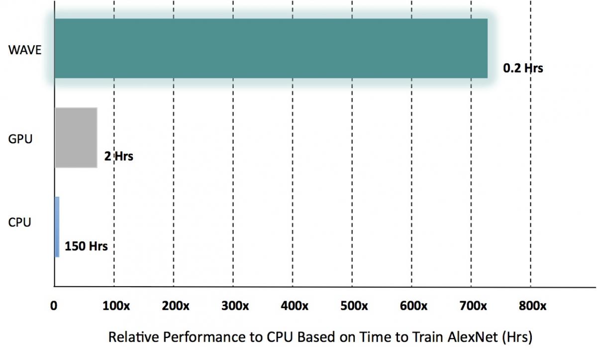
Figure 4. Wave Computing believes that its DPU (in a sixteen-chip configuration in this particular case) will perform strongly versus alternatives such as a NVIDIA DGX-1 with 8 P100 GPUs, and an Intel Intel Xeon E5-2697 v3 CPU, when training deep learning models such as AlexNet. The simulation forecasts shown, sourced by the company, await first silicon for confirmation; equally unknown at this point is relative performance versus CPUs and GPUs on other models as well as across various deep learning frameworks.
For now, Wave Computing will operate as a system supplier, selling sixteen DPU-based 3U form factor rack units priced equivalent to (but with claimed performance significantly higher than) the NVIDIA DGX-1 deep learning system at approximately $129,000. In the future, however, Wave Computing plans to broaden its offerings, also becoming a chip supplier and offering a range of DPU SoC sizes focused not only on deep learning model training applications but also lower-end, lower-PE count chips targeting inference opportunities. To this end, Kim claims that "We feel we can inference effectively everything but the very lowest power consumption applications, where any off-chip memory is verboten."
Add new comment