
Last month's announcement by Advanced Micro Devices that its "Bulldozer"-based Opteron microprocessors for servers had begun shipping to customers for revenue, followed by last week's release of first public benchmarks for Bulldozer-based AMD FX CPUs, capped off a year-long series of new CPU microarchitectures and devices for the company. Notably, the microarchitectures represent the first fresh offerings from AMD since 2007's K10 microarchitecture, which first appeared in "Barcelona" CPUs for servers and "Phenom" for desktops.
Intel's "tick tock" strategy has yielded several new microarchitecture iterations (and dozens of derived products) since 2007, so a robust competitive response from AMD was necessary to ensure the company's continued relevance in the x86 market. And after many years of promoting the "Fusion" single-chip CPU-plus-GPU concept, beginning in mid-2006, AMD was overdue to translate hype into silicon reality.
Simple First
First to arrive on the scene was the "Bobcat" core, unveiled in conceptual form (PDF) at the August 2010 Hot Chips conference (Figures 1 and 2):
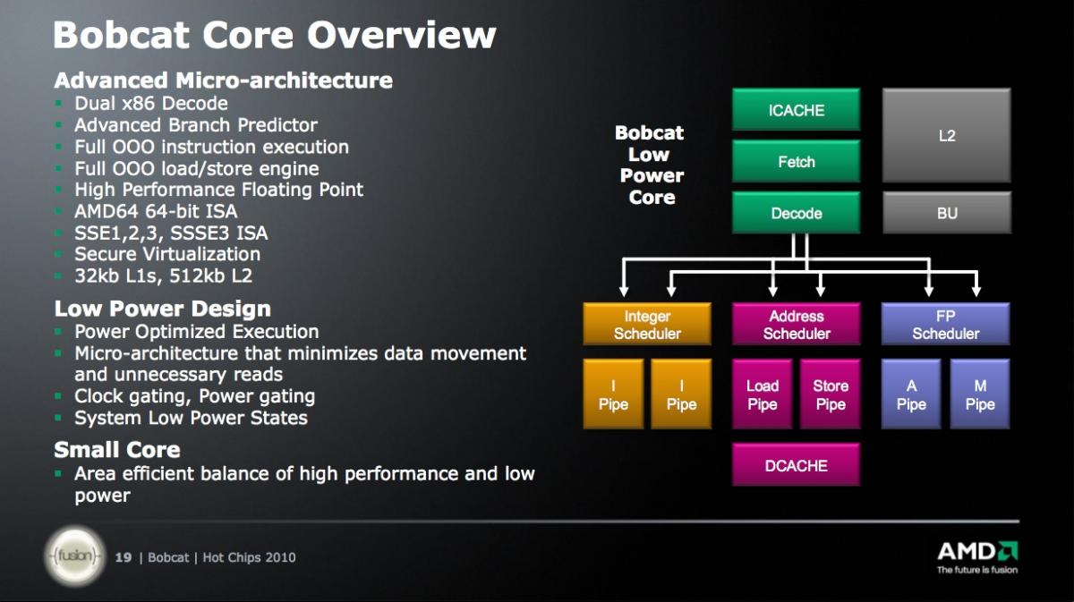
Figure 1. Bobcat one-ups Intel's "Atom" with out-of-order instruction execution capabilities.
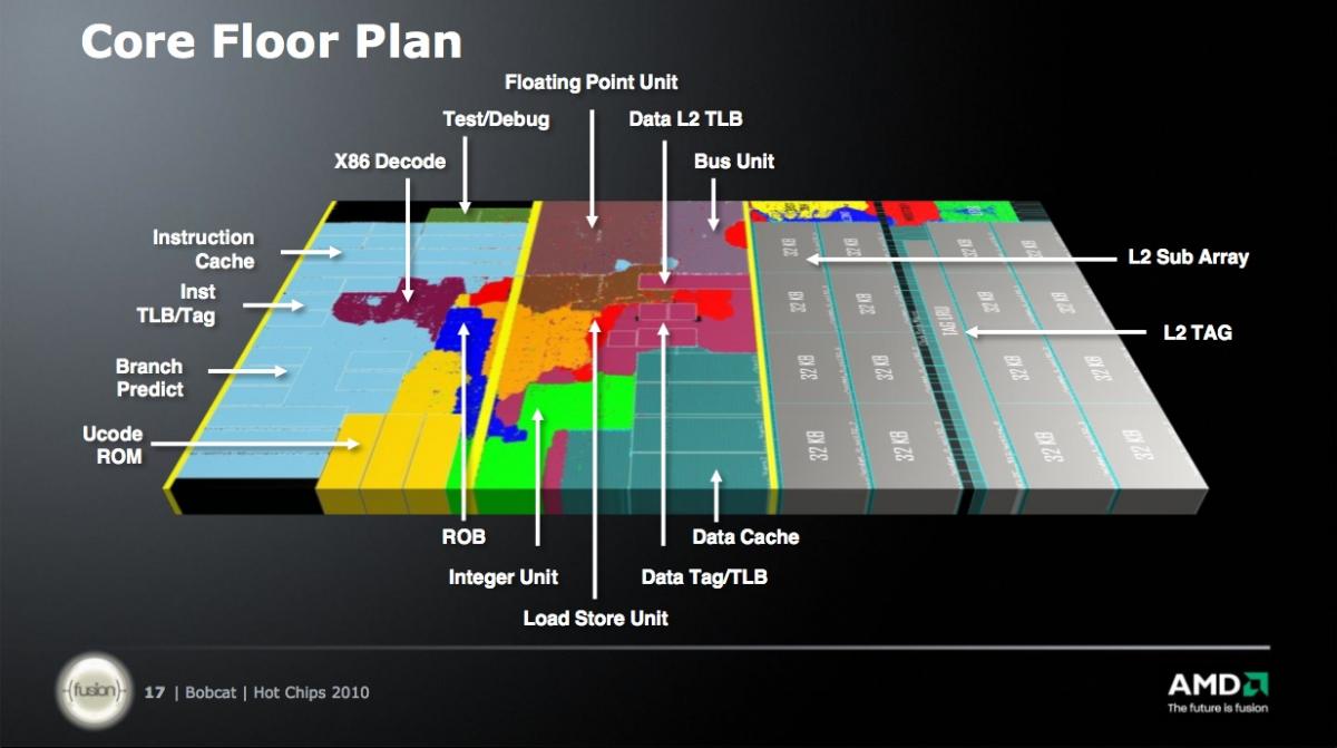
Figure 2. Bobcat's synthesizable core enables foundry portability and quick-turn SoC design.
One month later, I benchmarked a functional Bobcat-based CPU prototype at AMD's hotel suite down the street from the Intel Developer Forum; guerilla marketing at its finest. And AMD formally unveiled the first Bobcat-based products at the January 2011 Consumer Electronics Show (Figure 3):
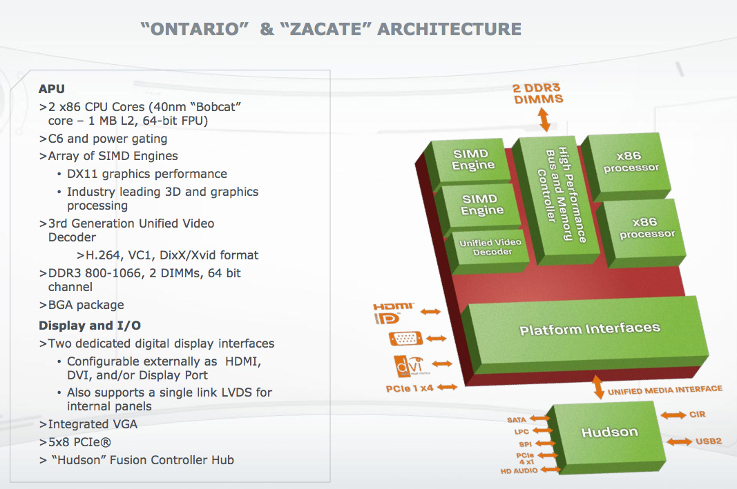
Figure 3. Bobcat-based "Ontario" and "Zacate" finally translated AMD's longstanding Fusion aspirations into reality; the SIMD engines in the upper left corner are the GPU.
Bobcat is a synthesizable core, which provides AMD both foundry flexibility and the ability to rapidly implement SoCs, at the cost of reduced silicon efficiency versus the full custom designs typically tackled by Intel. As you might already be able to tell from the presentation screenshots above, cost-optimized entry-level systems are the primary Bobcat target, finally giving AMD a credible conceptual competitor to Intel's Atom, which was first introduced in the spring of 2008. While Bobcat doesn't support Atom's per-physical-core "HyperThreading" simultaneous multithreading scheme, it makes two notable and related feature set advancements beyond today's Atom products: out-of-order instruction reordering, and physical rename registers to save power.
Like Atom, Bobcat supports MMX (multimedia extension) instructions along with SSE (streaming SIMD extension) instruction set generations 1 through 3. As such, neither architecture currently comprehends Intel's various SSE4 instruction set sub-generations or AVX (the 256-bit floating-point Advanced Vector Extensions instruction set implemented for the first time in Intel's "Sandy Bridge" CPUs). Look at Figure 3 again, and you'll see two additional SIMD blocks in the Bobcat-based SoC block diagram, in the upper left corner. They represent the integrated GPU (graphics processor), which AMD has renamed an APU (accelerated processing unit) befitting AMD’s Fusion-era intent that the GPU be used not only for graphics, but also for other data-parallel tasks. The 9 watt Ontario (Fusion C-Series) variants of the first-generation Bobcat-based SoCs, fabricated on a 40 nm process, contain a 280 MHz Radeon HD 6250 graphics core. The 18 watt Zacate (Fusion E-Series) versions embed a 500 MHz Radeon HD 6310 GPU. Both GPUs offer 80 unified (vertex, geometry and/or pixel) shaders, capable of tackling a variety of integer and floating-point math functions.
So-called GPGPU (general-purpose computing on graphics processing units) is a concept likely already familiar to those of you who've been closely following AMD (and ATI Technologies, which AMD acquired in late 2006) or NVIDIA. It refers to leveraging the massively parallel processing capabilities of a GPU as a CPU co-processor. Historically, GPGPU has found use in accelerating various still image and video-processing functions, as well as for more specialized applications such as encryption and decryption, virus scanning, and supercomputer database analytics. The migration of the CPU-to-GPU hardware interface beyond predominantly unidirectional PCI to AGP and (especially) PCI Express has been beneficial in this regard, and an on-chip optimized link between the two cores is better yet, at least conceptually. Equally encouraging has been the software API migration beyond vendor-proprietary Stream (AMD) and CUDA (NVIDIA) to industry-standard OpenCL and DirectX Compute.
A Fusion-Augmented Evolution
Next to get the Fusion treatment was "Llano", whose die is shown in the presentation slide below (Figure 4):
Figure 4. AMD devoted roughly half of the Llano die to on-chip graphics, versus a substantially lower percentage with Intel's Sandy Bridge.
Lest you doubt AMD's dedication to the Fusion concept, note that the entire bottom half of the die pictured in Figure 4 is the GPU. Llano is based on AMD's "Stars" core, a 32 nm shrink of the Phenom II containing two, three or four integer-plus-floating point core combos, but without Phenom II's L3 cache. In its place is an integrated graphics core that (as with Bobcat) is based on "Evergreen" Radeon HD 6000-series technology. In this case, however, the GPU includes either 160, 320 or 400 unified shaders, depending on the specific product variant, and runs at speeds up to 600 MHz. Like Phenom II, Stars comprehends Intel-compatible MMX, SSE, SSE2 and SSE3 SIMD instruction sets, along with AMD's proprietary SSE4a.
A Core-Redefining Revolution
First Llano models (formally known as the Fusion A-Series) began shipping in June, with additional variants following in August and September. Take a look at AMD's published desktop and mobile roadmaps from January, however, and you'll note that Llano has a rather short forecasted lifetime, with 2012 devoted to Bobcat- and Bulldozer-based devices (Figures 5 and 6).
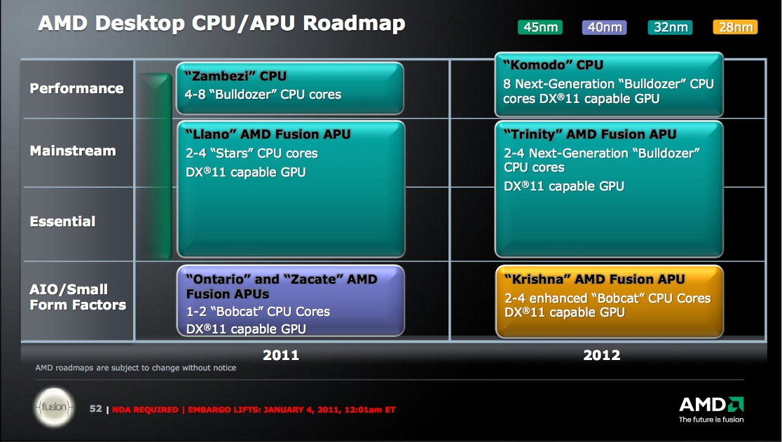
Figure 5. AMD's near-term desktop CPU roadmap reveals that Llano (and its K10 microarchitecture foundation) will have a short life.
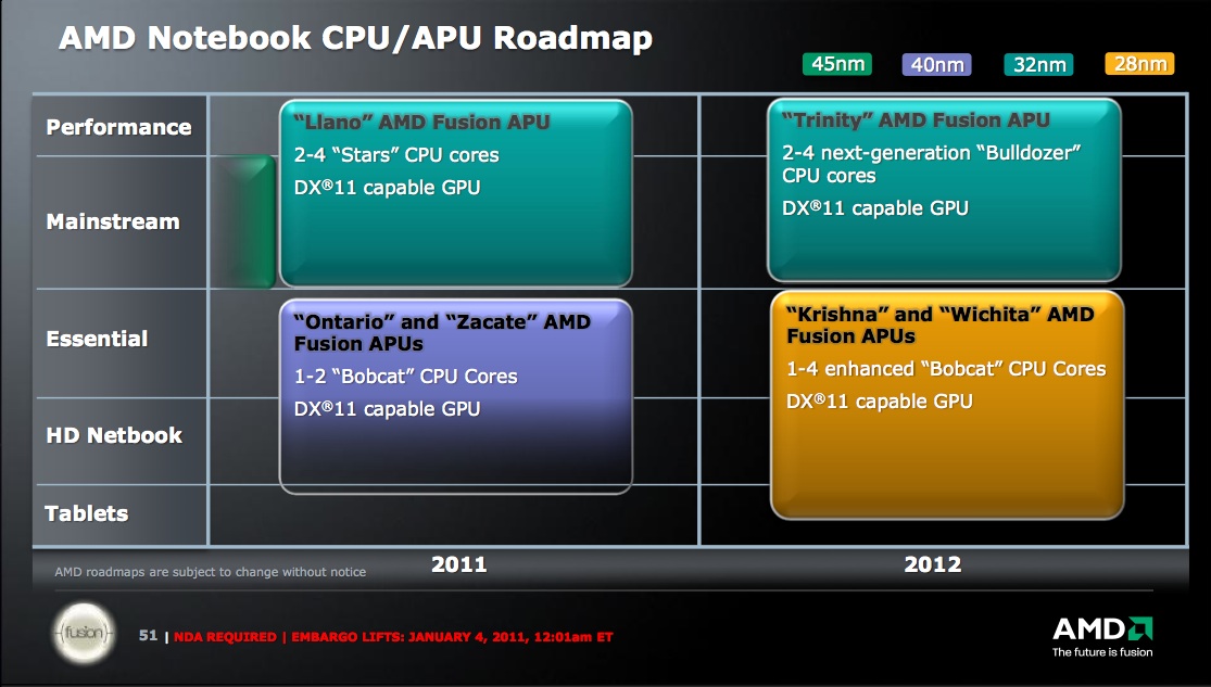
Figure 6. Bulldozer gets on-die graphics in 2012.
Bulldozer is, for 2011, a server- and desktop-exclusive CPU. In its first-generation iteration, it doesn't contain an on-chip GPU; there simply isn't enough silicon area cost-effectively available on the die. And AMD has made at least one other notable silicon-slimming move, as the block diagram below highlights (Figure 7):
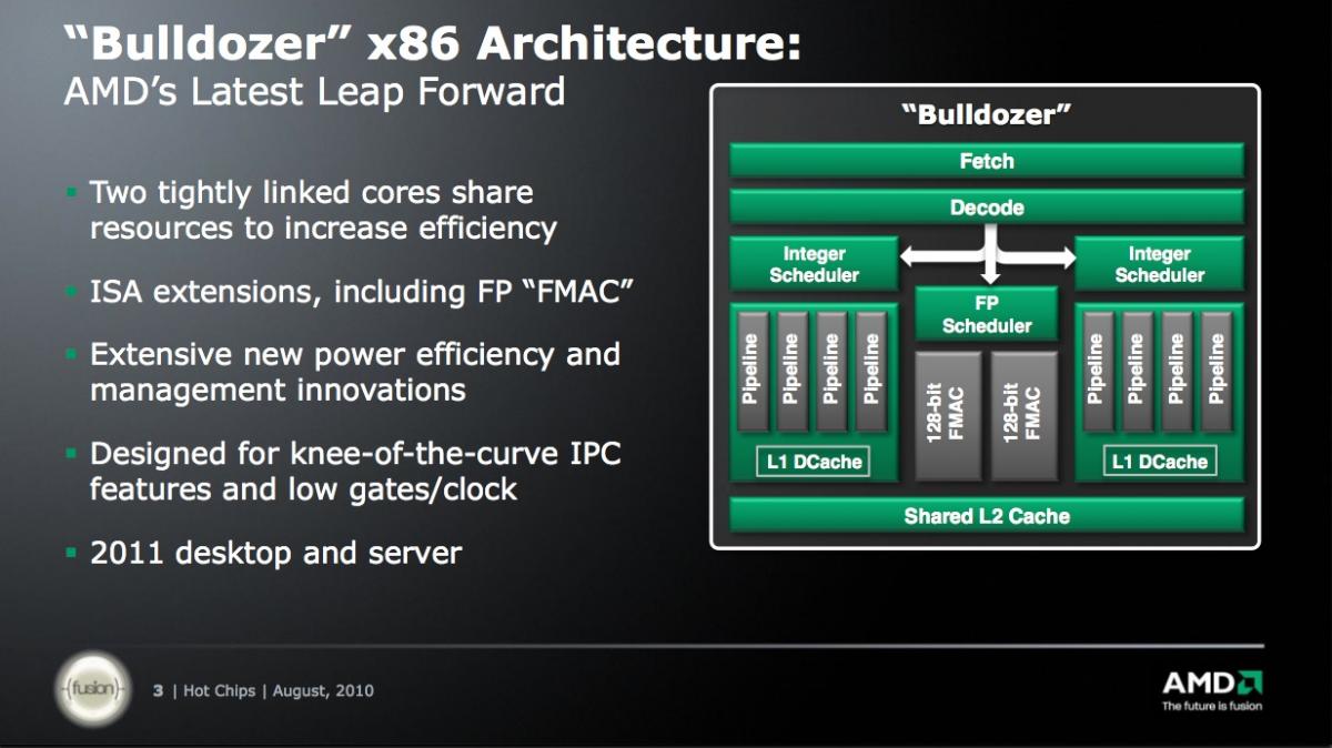
Figure 7. The Bulldozer module redefines the concept of an x86 CPU core.
Ever since 1989 and Intel's 486DX, which for the first time brought floating-point co-processor capabilities on-board the CPU, a consistent 1:1 ratio between integer and floating point cores had existed across all x86 processor suppliers. Befitting that fact, the "core" atomic unit terminology evolved in short order to encompass the integer-plus-floating point combination. With Bulldozer, AMD takes a fairly radical forward (or, depending on your perspective, backward) step. Each "module" atomic unit contains two integer units bolted to a single 128-bit floating-point core. So keep in mind going forward that when AMD marketing tells you (for example) that the upcoming Opteron 6200 series (code-named "Interlagos") contains up to 16 cores, the reference is to integer cores; the floating-point core count is half that metric.
AMD discussed the Bulldozer architecture in some detail (PDF) at both this and last year's Hot Chip Conferences, held in late August 2010 and mid-August 2011. From a digital signal processing standpoint, Bulldozer implements the following SIMD instruction sets:
- MMX
- SSE
- SSE2
- SSE3
- SSE4.1
- SSE4.2, and
- AVX
Note that AMD's formerly proposed SSE5 instructions are not on the list. Subsequent to their unveiling in August 2007, they (unsurprisingly) did not receive support from Intel and were therefore deprecated. AMD has replaced them with the XOP, FMA4, and CVT16 instructions, which retain SSE5 proposed functionality but have better compatibility with Intel's AVX coding scheme. Note, too, that the above roadmap slides show second-generation Bulldozer-based products with on-die GPUs appearing in 2012.
The consumer desktop variant of Bulldozer is the AMD FX, and as mentioned at the beginning of this article, the nondisclosure restrictions on published benchmarks for it expired last week, prompting a flurry of detailed reports from various PC enthusiast sites. Unfortunately for AMD, the early statistics aren't encouraging, either in an absolute sense or relative to Intel counterparts or even AMD K10 microarchitecture-based predecessors. A high-end AMD FX is hard-pressed to keep pace with a mid-range Sandy Bridge CPU, far from a high-end Intel competitor, except in a few benchmarks that are both heavily threaded and integer-centric (reminiscent of server usage scenarios, thereby giving AMD some near-term hope).
A variety of theories have been proposed to explain the underwhelming results; the CPUs weren't seemingly able to hit their originally forecasted clock speeds, for example, within reasonable power consumption limits. L1 and L2 cache access latencies are also quite long, and while the front end of each module's processing pipeline can decode four instructions per clock (versus three with K10), each instruction decoder is now servicing two integer cores, not one. Finally, AMD reports that the thread scheduler built into Windows 7 isn't optimized for Bulldozer's module-based architecture; Windows 8 will reportedly make improvements in this regard, and Linux O/Ss will likely also be able to respond quickly with optimizations. Finally, as the Figure 5 and 6 roadmaps suggest, next-generation Bulldozer successors will hopefully learn from and improve on today's offerings. Then again, Intel has 22 nm-based "Ivy Bridge" poised to ramp into production in the next few months, and the company was even showing functional systems based on its successor, "Haswell", at last month's Intel Developer Forum.
Conclusion
For some time now, a heated debate has raged as to whether (and if so, where) standalone DSP chips are still necessary, versus user-programmable hardware in the form of FPGAs and software running on general-purpose CPUs and GPUs. AMD's latest product offerings may further complicated DSP suppliers' aspirations, both by virtue of their increasingly robust SIMD integer and floating point facilities and their on-die GPGPU capabilities. Then again, DSPs aren't standing still, either. How do you handicap this particular race, both short- and long-term?
Add new comment