
Altera recently disclosed architecture details of its next generation Stratix V FPGA family. The architecture features a variable-precision DSP block, designed to provide better resource utilization for algorithms requiring a variety of data widths. Altera represents this approach via a variable precision “dial,” shown in Figure 1. In addition to 18-bit by 18-bit (18×18) and 36×36 modes supported by previous blocks, the DSP block natively supports three 9×9 multiply operations or one 18×25 or 18×36 multiply. The multiplier also supports single-precision floating-point mantissa multiplication, implementing 27×27 multiply without external logic. The Stratix V architecture, implemented using TSMC 28 nm technology, is targeted at high-end applications such as telecom and wireless, military, broadcast, medical, and test and measurement equipment.
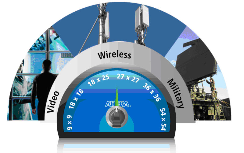
Figure 1: Variable Precision Dial
Compared to previous Altera and Xilinx DSP blocks, which rely on 18×18 multipliers, the new Altera DSP block architecture provides finer granularity to enable more efficient use of resources, tuned to the needs of an particular algorithm. Table 1 shows the number of each size of multiply operation that can be performed at one time by the new DSP block. High-precision formats (36×36 and 54×54) require more than one multiply block, as was the case with previous architectures. Support for the 9×9 multiply should increase the total number of multiplies available on a single chip for applications such as video which use small data sizes. Support for 27×27 multiplications, which effectively consumes two 18×18 multipliers, would have previously required four 18×18 multipliers in Altera or Xilinx FPGA families. In order to support the new higher-precision modes, Altera has increased the size of the accumulator and cascading logic from 48 bits to 64 bits.
|
Multiply input size (bits) |
Multiplies per DSP block |
Typical uses |
|
9×9 |
3 |
Video processing |
|
18×18 |
2 |
Medium-precision fixed-point operations |
|
18×25 |
1 |
FFT (higher precision intermediate data) |
|
18×36 |
1 |
FFT (higher precision intermediate data), high-precision coefficients |
|
27×27 |
1 |
Medium-precision fixed-point operations Single-precision floating-point mantissa multiplication |
|
36×36 |
½ (2 blocks required) |
High-precision fixed-point |
|
54×54 |
¼ (4 blocks required) |
Double-precision floating-point mantissa multiplication |
Table 1: Supported Multiply Modes
Other new aspects of the Altera DSP block architecture, compared with the DSP block in the Stratix-IV architecture, include a pre-adder and an internal coefficient register bank. The pre-adder allows symmetric FIR filters to use a single multiplication to compute two filter “taps” using two data values which rely on the same coefficient. This structure¾which already exists in the Xilinx DSP block¾could be implemented with external logic in previous Altera devices, but can now be handled more efficiently inside the DSP block. The internal coefficient register bank supports up to sixteen 18-bit coefficients or eight 27-bit coefficients, which can be addressed in an arbitrary fashion. Smaller filters or filters distributed across several DSP blocks should be able to use these internal register banks for coefficient storage, eliminating the need for registers or memory blocks and the associated routing logic.
According to Altera, the largest DSP-targeted Stratix V device will include 1,840 DSP blocks, which Altera expects to run at 500 MHz. With two 18×18 multipliers per block, the device should be capable of a peak of 1,840 18-bit GMACS using the DSP blocks. Hardware designers will be able to access the DSP block’s variable-precision modes through the existing Quartus synthesis flow using HDL coding techniques or using Altera’s MegaWizard tool to create multiplier modules with the desired precision. Altera will provide coding templates showing how to ensure that the synthesis tool takes advantage of new features like the pre-adder and coefficient register bank.
One other notable architectural enhancement in the Altera Stratix V family is an “Embedded HardCopy Block.” This is a metal-programmed gate array block embedded alongside the traditional SRAM-based FPGA fabric. It allows Altera to create smaller, higher-performance implementations of fixed-function blocks. The HardCopy block is located close to the I/O ring, and is primarily expected to be used for new I/O standards and I/O related processing. It will not be appropriate for implementation of an embedded CPU, so the synthesizable NIOS processor core will remain the supported CPU in this family.
Altera’s white paper states that the new DSP block’s variable-precision architecture will “allow the designer to set the precision mode to match the algorithm instead of the other way around”. Ultimately, it will contribute to the silicon efficiency of DSP applications implemented in Stratix V FPGAs, which is an increasingly important consideration as FPGAs find more widespread use as DSP engines.
Additional details of the Stratix V FPGAs, which are expected to begin shipping in Q1 2011, are available here.
Add new comment